Introduction
PCB size tolerances play a critical role in the success of printed circuit board fabrication and assembly processes. These tolerances define the acceptable variations in PCB dimensions, ensuring that boards fit precisely into enclosures, align with components, and maintain electrical performance. Inaccurate dimensions can lead to assembly failures, mechanical stress, or reliability issues in the field. For electric engineers, grasping PCB manufacturing tolerances is essential for specifying designs that balance performance with manufacturability. This article explores PCB size tolerances, their influencing factors, industry standards, and quality control measures to achieve consistent PCB fabrication outcomes. By understanding these elements, engineers can optimize designs for reliable production.
What Are PCB Size Tolerances and Why Do They Matter?
PCB size tolerances refer to the permissible deviations in overall board dimensions, including length, width, thickness, and outline contours from the nominal design specifications. These include routing tolerances for edges, panel size variations, and flatness metrics like bow and twist. PCB dimensions must stay within these limits to prevent mismatches during integration into systems. In high-volume production, even minor deviations accumulate, affecting yield and cost.
The importance of PCB manufacturing tolerances becomes evident in assembly stages. Precise PCB dimensions ensure proper component placement, especially for surface mount technology where alignment is critical. Tolerances impact signal integrity by influencing impedance control and thermal management. Poor adherence leads to rework, delays, or field failures, underscoring the need for robust quality control in PCB fabrication. Engineers must consider these tolerances early in design to avoid costly iterations.
Factors Influencing PCB Dimensions During Fabrication
Several factors contribute to variations in PCB size tolerances during manufacturing. Material properties, such as coefficient of thermal expansion in laminates, cause dimensional changes under heat from lamination or soldering. Routing and scoring processes introduce mechanical tolerances based on tool precision and machine calibration (see our detailed guide on PCB outline tolerances). Multilayer boards experience additional stresses from layer registration and via drilling alignment.
Thermal cycling in fabrication, including baking and reflow simulation, exacerbates warpage, altering effective PCB dimensions. Panel size and layout affect uniformity, as edge effects differ from center regions. Copper distribution imbalances lead to bow and twist, distorting flatness. Factory-driven insights reveal that controlling these factors through process optimization maintains PCB quality control.
Industry Standards for PCB Manufacturing Tolerances
Industry standards provide the framework for PCB size tolerances, ensuring consistency across fabricators. IPC-6012 outlines qualification and performance specifications for rigid printed boards, defining acceptability criteria based on product classes. Class 1 offers basic tolerances for general use, while Class 2 and Class 3 impose progressively stricter limits for dedicated service and high-reliability applications. These classes guide PCB dimensions, with Class 3 demanding enhanced precision for aerospace or medical uses (compare with our standard PCB dimensions guide).
IPC-A-600 complements this by specifying visual and dimensional acceptability attributes post-fabrication. Standards emphasize measurement methods for outline, thickness, and flatness to verify compliance. Adhering to these prevents deviations that compromise PCB fabrication reliability.
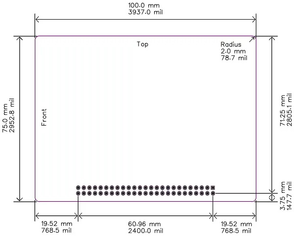
Key Aspects of PCB Dimensions: Outline, Thickness, and Flatness
Board outline tolerances encompass edge routing accuracy, critical for mechanical fit. Variations here arise from spindle runout or bit wear, necessitating controlled feeds and speeds. Engineers specify tolerances in design files, accounting for process capabilities.
PCB thickness tolerances relate to laminate stackup, copper foils, and prepreg variations. Uniform pressing maintains nominal values, vital for connector mating and wave soldering clearance. Deviations affect high-frequency performance by altering dielectric spacing.
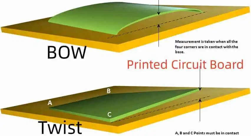
Flatness, including bow and twist, measures deviation from planarity. IPC-6012 sets limits tighter for surface mount boards to ensure pick-and-place accuracy. Warpage from asymmetric copper or bake-out influences assembly yields.
Quality Control Measures in PCB Fabrication
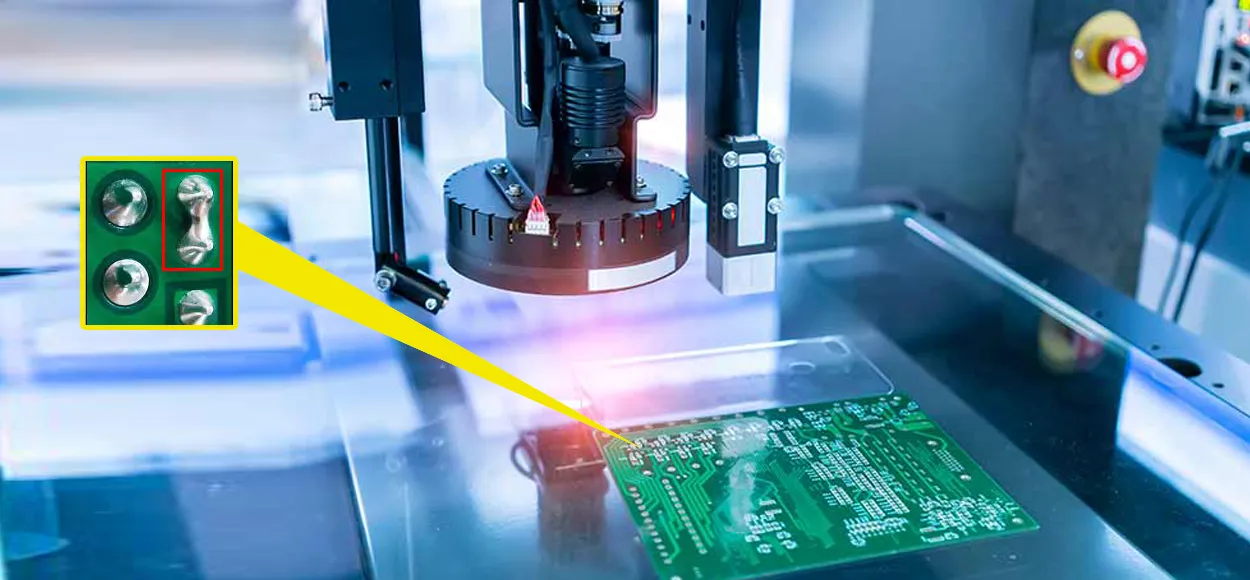
Effective PCB quality control begins with incoming material inspection for dimensional stability. Automated optical inspection verifies outline and fiducial marks pre-routing. Post-milling, coordinate measuring machines gauge PCB dimensions against Gerber data.
Thickness profiling uses micrometers at multiple points, flagging stackup inconsistencies. Flatness checks employ IPC-TM-650 methods, such as dial indicators on fixtures. Statistical process control tracks tolerances across panels, enabling real-time adjustments. Factory protocols align with standards to minimize scrap.
Traceability through serial numbers links measurements to lots, supporting audits. Engineers review control charts for trends in PCB manufacturing tolerances.
Best Practices for Achieving Accurate PCB Dimensions
Designers incorporate margin in PCB dimensions, specifying tolerances per class needs. Balanced copper distribution on layers counters warpage risks (learn more in our DFM guidelines). Fiducials aid alignment in routing and assembly.
Select materials with matched CTE for multilayers. Simulate thermal profiles to predict distortions. Specify routing tabs or vacuum fixturing for thin panels.
In fabrication, calibrate routers daily and use compensation for tool deflection. Controlled baking reduces moisture-induced bow. Post-process beveling or scoring demands precise depth control.
Collaboration with fabricators refines specs, ensuring PCB quality control.
Common Challenges and Troubleshooting in PCB Size Tolerances
Warpage tops challenges, often from uneven curing or copper asymmetry. Troubleshooting involves symmetric stackups and constrained lamination. Outline oversize signals dull tools; refresh bits promptly.
Thickness variation points to prepreg flow issues; adjust resin content. Flatness failures post-soldering trace to inadequate bake-out; extend dwells. Data logs pinpoint root causes for corrective actions.
Conclusion
Mastering PCB size tolerances ensures seamless manufacturing and deployment. From standards like IPC-6012 to hands-on quality control, attention to dimensions drives reliability. Electric engineers benefit by integrating these insights into designs, minimizing risks in PCB fabrication. Prioritizing tolerances enhances overall product quality, supporting efficient production scales.
FAQs
Q1: What are standard PCB size tolerances for Class 2 boards?
A1: PCB size tolerances for Class 2 boards follow IPC guidelines, focusing on outline, thickness, and flatness suitable for general electronics. Factory processes achieve consistent PCB manufacturing tolerances through calibrated routing and lamination. Specify requirements in design to align with fabricator capabilities, ensuring PCB quality control.
Q2: How does warpage affect PCB dimensions?
A2: Warpage distorts PCB dimensions, impacting assembly alignment and component reliability. It arises from thermal stresses and material imbalances during fabrication. Standards dictate maximum allowable bow and twist, with quality checks verifying compliance. Balanced designs and process controls mitigate effects on PCB size tolerances.
Q3: Why are PCB manufacturing tolerances critical for electric engineers?
A3: PCB manufacturing tolerances ensure precise dimensions for signal integrity and mechanical fit. Deviations compromise performance in high-speed circuits. Engineers reference standards to specify tolerances, aiding PCB fabrication success. Proactive quality control prevents costly revisions.
Q4: How to measure PCB dimensions accurately?
A4: Measure PCB dimensions using calipers for outline, micrometers for thickness, and fixtures for flatness. Optical systems provide non-contact verification of tolerances. Align with IPC methods for PCB quality control. Regular calibration maintains accuracy in production.
References
IPC-6012E — Qualification and Performance Specification for Rigid Printed Boards. IPC, 2017
IPC-A-600K — Acceptability of Printed Boards. IPC, 2020


