Introduction
In high-speed PCB design, maintaining signal integrity has become a critical challenge as data rates continue to increase. Engineers face issues like signal distortion, attenuation, and crosstalk, which can compromise system performance. Low Dk PCB materials play a pivotal role in addressing these concerns by minimizing the dielectric constant impact on signal propagation. These materials reduce capacitance and improve signal velocity, essential for applications operating at multi-gigabit speeds. Selecting the right PCB material selection strategy ensures reliable high-speed PCB design outcomes. This guide explores the fundamentals of low Dk materials and their contributions to signal loss reduction.
Signal integrity directly affects the overall functionality of electronic systems, from telecommunications to computing hardware. Traditional materials often fall short at higher frequencies due to higher dielectric constants. Low Dk PCB signal integrity benefits stem from faster signal travel and lower losses. Engineers must understand the interplay between material properties and electrical performance to optimize designs effectively.
Understanding the Dielectric Constant (Dk) in PCB Materials
The dielectric constant, or Dk, quantifies a material's ability to store electrical energy in an electric field relative to vacuum. In PCBs, it influences the effective permittivity between conductors, affecting signal behavior. Lower Dk values allow signals to propagate closer to the speed of light in free space, reducing delays. This property becomes crucial as frequencies rise, where even small variations can lead to timing mismatches. Material composition, including resin and reinforcement fibers, determines the Dk value.
Dk measurements vary with frequency, temperature, and moisture content, requiring careful characterization. Standard test methods ensure consistency across suppliers. IPC-TM-650 provides detailed procedures for evaluating dielectric properties under controlled conditions. Engineers rely on these to predict material performance accurately.
Why Low Dk Materials Matter for Signal Integrity
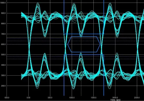
High-speed signals demand materials that preserve waveform quality over long traces. Higher Dk increases the capacitance per unit length in transmission lines, slowing signals and altering impedance. This leads to reflections and degradation in eye diagrams. Low Dk PCB signal integrity improves by enabling tighter timing budgets and better crosstalk isolation. Signal loss reduction becomes evident as attenuation decreases with lower permittivity.
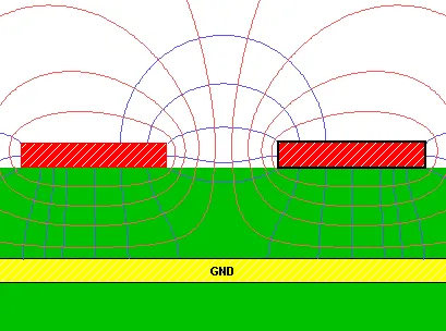
In multilayer boards, asymmetric Dk across layers can cause skew between signals. Uniform low Dk materials mitigate this issue, supporting differential pair routing. The dielectric constant impact extends to via transitions, where stub effects amplify at high frequencies. Choosing low Dk options aligns with the demands of modern high-speed PCB design.
The Dielectric Constant Impact on Signal Propagation and Loss
Signal velocity in a PCB trace follows the formula v = c / sqrt(Dk_eff), where Dk_eff accounts for the effective dielectric seen by the field. Lower Dk raises velocity, shortening propagation delays critical for synchronized data transfer. Impedance Z0 also depends on Dk, with formulas for microstrip and stripline geometries incorporating it directly. Mismatches from Dk variations cause reflections, distorting signals.
Attenuation arises from conductor loss, dielectric loss, and radiation, with dielectric loss tied to both Dk and dissipation factor (Df). While Dk primarily affects speed, its interaction with Df determines overall signal loss reduction. Low Dk materials often pair with low Df for optimal performance. Engineers model these effects using field solvers to predict behavior before fabrication.
Frequency dependence complicates matters, as Dk may decrease slightly at higher GHz ranges. Moisture absorption elevates Dk, exacerbating losses in humid environments. IPC-4101 specifications guide material qualification, ensuring stability across operating conditions.
Key Properties of Low Dk PCB Materials
Low Dk materials typically feature advanced resins with minimal polar components to lower permittivity. Reinforcement styles, such as low Dk glass fabrics, further optimize properties. These materials maintain mechanical strength while prioritizing electrical performance. Thermal expansion coefficients must match copper to prevent warpage during processing.
Dissipation factor complements Dk, as low Df minimizes energy conversion to heat. Together, they enable signal loss reduction in long traces. Stability over temperature ranges ensures consistent high-speed PCB design reliability. Engineers evaluate CTE, Tg, and Z-axis expansion alongside electrical specs.
Fabrication compatibility influences selection, including drillability and plating adhesion. Low Dk materials may require adjusted process parameters to avoid defects. IPC-6012E outlines qualification tests for rigid boards, verifying performance under thermal and mechanical stress.
PCB Material Selection Best Practices
Start with defining frequency, data rate, and trace lengths to gauge Dk needs. For signals above 1 GHz, prioritize materials with Dk below standard levels. Balance cost with performance, as low Dk options increase expenses. Consult datasheets for Dk vs frequency curves and Df values.
Hybrid stackups combine low Dk cores for signal layers with cost-effective prepregs elsewhere. This approach optimizes PCB material selection without full premium material use. Simulate stackup effects on impedance and loss using design software. Verify with time-domain reflectometry post-prototype.
Consider environmental factors like operating temperature and humidity. Materials with low moisture absorption preserve low Dk PCB signal integrity over time. Collaborate with fabricators early to confirm process windows.
Design Considerations for High-Speed PCBs with Low Dk Materials
Route critical signals on inner layers with uniform dielectric for symmetric fields. Use ground planes adjacent to signal layers to control impedance precisely. Minimize vias by planning routing paths efficiently. Backdrill stubs if necessary to reduce reflections.
Length matching for differential pairs accounts for Dk-induced delays. Controlled impedance tolerances tighten to 5% or better with low Dk. SerDes channels benefit from low Dk to extend reach without repeaters. Power integrity couples with signal design, as PDN impedance affects noise.
Test fabricated boards for insertion loss and return loss to validate simulations. Adjust designs iteratively based on measurements.See our detailed RF PCB design guide for layout best practices.
Conclusion
Low Dk PCB materials unlock superior signal integrity by mitigating dielectric constant impact on propagation and loss. Strategic PCB material selection enhances high-speed PCB design reliability and performance. Best practices in characterization, stackup planning, and routing ensure optimal outcomes. Engineers equipped with this knowledge can tackle demanding applications effectively. Prioritizing low Dk alongside low Df drives signal loss reduction across frequencies.
FAQs
Q1: What is the primary benefit of low Dk PCB signal integrity in high-speed designs?
A1: Low Dk materials increase signal velocity and reduce capacitance, minimizing propagation delays and impedance mismatches. This supports higher data rates with less distortion. In PCB material selection, they enable longer traces without excessive loss. Engineers achieve better eye opening and reduced jitter.
Q2: How does dielectric constant impact signal loss reduction?
A2: Higher Dk elevates effective permittivity, slowing signals and increasing attenuation when combined with Df. Low Dk lowers these effects, preserving amplitude over distance. High-speed PCB design relies on this for maintaining signal quality. Testing per industry standards confirms reductions.
Q3: Why consider both Dk and Df in PCB material selection?
A3: Dk governs speed and impedance, while Df dictates dielectric loss. Together, they determine overall signal loss reduction. Low values of both are essential for low Dk PCB signal integrity at GHz frequencies. Balanced selection prevents overheating and distortion.
Q4: What role do standards play in low Dk material evaluation?
A4: Standards like IPC-TM-650 provide test methods for accurate Dk measurement. They ensure reproducibility across materials and suppliers. This supports reliable high-speed PCB design decisions.
References
IPC-TM-650 2.5.5 — Test Methods Manual for Dielectric Constant Characterization. IPC.
IPC-4101E — Specification for Base Materials for Rigid and Multilayer Printed Boards. IPC, 2017.
IPC-6012E — Qualification and Performance Specification for Rigid Printed Boards. IPC, 2017.


