Introduction
IPC-6012 establishes the qualification and performance specifications for rigid printed boards in PCB manufacturing. This standard plays a pivotal role in defining critical parameters like IPC-6012 hole plating and via plating thickness, which directly influence plated through-hole integrity and overall PCB reliability. Engineers rely on these guidelines to ensure boards withstand operational stresses such as thermal cycling and mechanical vibration. Insufficient plating thickness can lead to electrical opens, signal degradation, or premature failures in high-density interconnects. Understanding these requirements helps optimize designs for consistent performance across production runs. This article delves into the specifics, drawing from factory perspectives on compliance and quality control.
What IPC-6012 Means for Hole and Via Plating
IPC-6012 outlines performance classes for rigid PCBs, categorized into Class 1 for general electronics, Class 2 for dedicated service reliability, and Class 3 for high-reliability applications. Hole plating thickness refers to the copper deposit on the walls of drilled holes, including plated through-holes (PTH) and vias, measured as an average per side. Via plating thickness follows similar criteria but varies slightly for microvias or blind/buried types. These thicknesses ensure robust electrical conductivity, adhesion to the dielectric, and resistance to barrel cracking under stress. In the manufacturing of IPC 6012 for HDI PCB, thin plating compromises reliability, leading to issues like electromigration or void formation during soldering. Factory data consistently shows that adhering to these specs reduces field failures by maintaining structural integrity in multilayer boards.
The relevance extends to modern high-speed designs where signal integrity demands uniform plating to minimize impedance variations. Plated through-holes carry power and ground signals, while vias interconnect layers, both requiring precise thickness for low resistance paths. Non-compliance risks delamination or cracking, especially in thick boards with aspect ratios exceeding 10:1. Engineers specifying Class 3 boards prioritize these metrics for aerospace or medical applications, where downtime is unacceptable. Overall, IPC-6012 hole plating guidelines bridge design intent with manufacturability, fostering long-term PCB reliability.
Technical Principles of Hole and Via Plating in IPC-6012
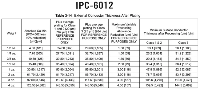
The plating process begins with electroless copper deposition to create a conductive seed layer, followed by electrolytic plating to build the required thickness. IPC-6012 specifies minimum average hole wall plating thicknesses to account for process variations. For Class 2 boards, the minimum average is 20 μm (0.8 mil) for PTH and most vias, while Class 3 demands 25 μm (1.0 mil) to enhance durability. Surface plating matches these values, ensuring consistent conductivity across features. Microvias, such as blind or buried types greater than two layers, align with PTH requirements, but cap plating for vias-in-pad is at least 12 μm (0.472 mil) in Class 3. See proven via plating techniques for deeper insight.
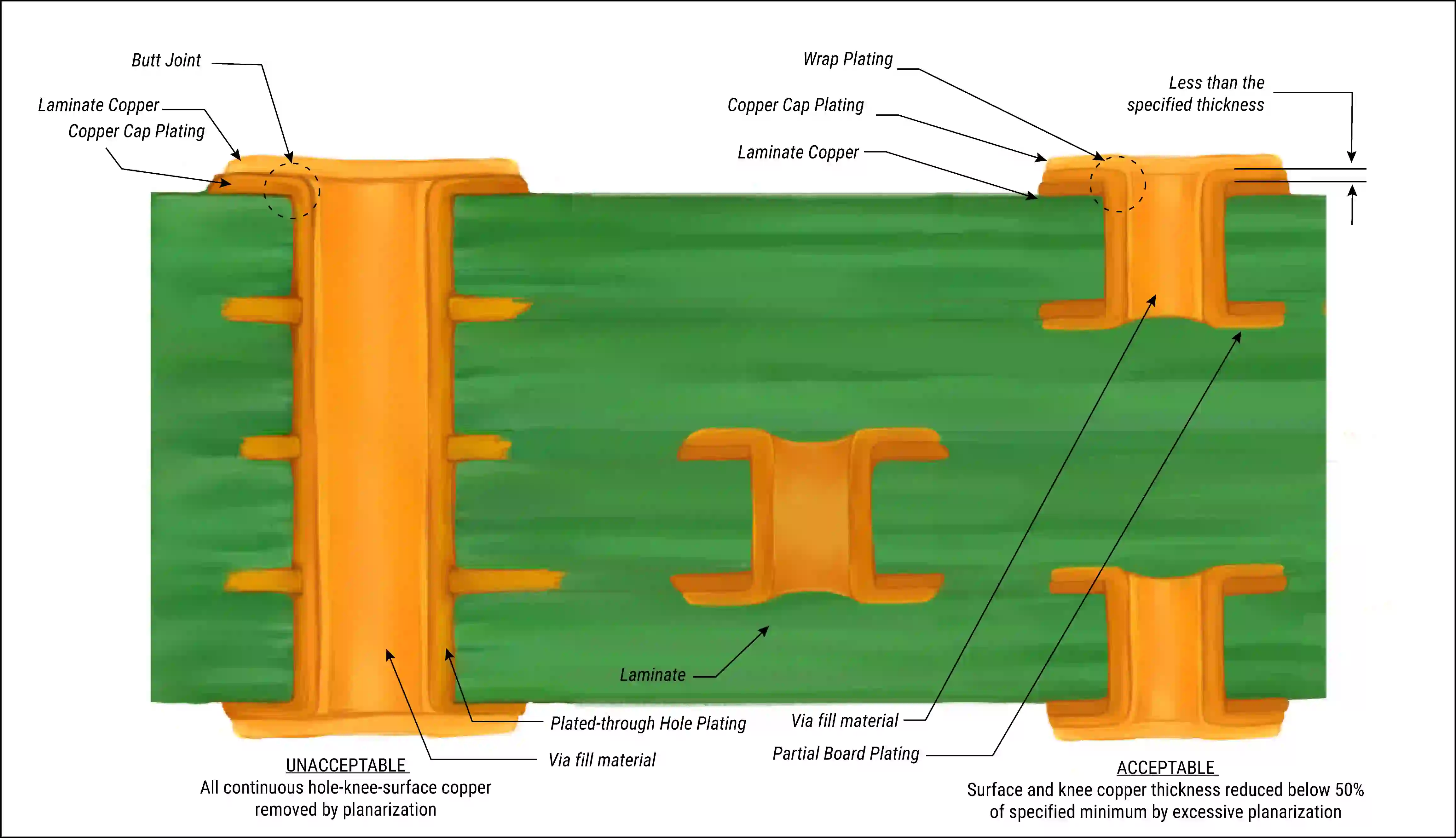
Wrap plating, or the copper extension over the hole edge onto the surface, prevents exposed dielectric and is governed by specific tables in the standard. Voids in plating are tightly controlled: Class 2 permits limited voids totaling no more than 5% of hole length, while Class 3 prohibits multiple voids for uninterrupted coverage. These principles stem from microsection evaluations, where thickness is averaged excluding glass fiber protrusions. Factories measure plating post-processing, as etching and plating sequences affect final dimensions. Table 3-4 through 3-6 in IPC-6012 detail these by feature type, emphasizing average over absolute minimums at any point.
| Feature | Class 2 Minimum Average (μm/mil) | Class 3 Minimum Average (μm/mil) |
|---|---|---|
| Hole Wall (PTH/Vias >2 layers) | 20 / 0.8 | 25 / 1.0 |
| Surface Plating | 20 / 0.8 | 25 / 1.0 |
| Microvia Cap Plating | Varies by table | 12 / 0.472 (min) |
This table summarizes core requirements, aiding quick reference in design reviews. External layers often include base foil plus plating, with totals like 48 μm minimum for Class 2 after processing.
Plating Processes and Factors Influencing Thickness in PCB Manufacturing
Electrolytic plating uses current density, bath chemistry, and time to deposit copper uniformly inside holes. High aspect ratios challenge throwpower, the ability to plate deep holes evenly, often requiring pulse plating or additives. Pre-plating desmear removes resin smear from drilling, ensuring adhesion. Factories monitor pH, temperature, and copper ion concentration to hit target thicknesses without nodules or dog-boning, where top plating thickens excessively.
Post-plating, flash etching levels surfaces, but over-etching risks thinning hole walls. IPC-6012 accounts for these by specifying post-process minimums. For filled vias, cap plating protrusion is limited to 50 μm to avoid solder wicking issues. Blind vias demand precise sequential plating to maintain sidewall coverage. Quality control involves inline X-ray for plating uniformity before final lamination.

Inspection Methods for IPC-6012 Plating Compliance
Microsectioning remains the gold standard for verifying via plating thickness, involving mounting, polishing, and microscopic measurement at multiple points. IPC-6012 requires evaluation on qualification lots, with acceptance based on average thickness across sections. Automated optical inspection detects surface voids, but cross-sections confirm internal plating. Electrical testing, like continuity checks under thermal stress, indirectly validates plating integrity.
For high-volume production, statistical process control tracks plating metrics against CpK values. Class 3 boards undergo 100% microsectioning on first articles. Common defects include knitline cracks from poor throwpower, addressed by process tweaks. These methods ensure plated through-hole reliability from fab to assembly.
Best Practices and Troubleshooting for Optimal Plating Thickness
Select plating vendors with proven Class 3 capabilities, specifying IPC-6012 compliance in purchase orders. Optimize drill sizes to lower aspect ratios, improving plating uniformity. Use simulation tools to predict throwpower before panels enter the line. Post-plating bake stabilizes copper, reducing hydrogen embrittlement risks.
Troubleshooting thin plating often traces to low current density or depleted baths; remedy with frequent analysis. Voids signal air entrapment or poor activation, fixed by enhanced rinsing. For via plating thickness inconsistencies, segment plating cycles for blind vias. Factories implement SPC charts for real-time adjustments, minimizing scrap.
Barrel fill for soldered PTHs requires 50% minimum for Class 2 and 75% for Class 3, verified via dye-and-peel or vertical microsections. These practices directly boost PCB reliability in demanding environments.
Case Insights: Common Plating Failures and Lessons from Production
In one factory scenario, Class 3 boards failed thermal cycling due to 18 μm average hole plating, below the 25 μm threshold, causing barrel cracks. Root cause was inadequate desmear, leading to poor seed adhesion. Corrective action involved extending permanganate etch times, achieving consistent thicknesses. Another issue arose in high-aspect vias, where dog-boning reduced effective plating; pulse-reverse plating resolved it.
These cases highlight the need for design-for-manufacturing reviews early. Engineers specifying tight via plating thickness should allocate margins for process etch-back. Production yields improved 15% post-implementation, underscoring standard adherence.
Conclusion
IPC-6012 hole plating and via plating thickness requirements form the backbone of reliable PCB manufacturing. Class-specific minimums of 20 μm for Class 2 and 25 μm for Class 3 ensure electrical and mechanical robustness in plated through-holes and vias. By mastering plating processes, inspection, and best practices, factories deliver boards that excel under stress. Designers and engineers benefit from these guidelines to balance performance with cost. Prioritizing compliance enhances PCB reliability across applications.
FAQs
Q1: What is the minimum via plating thickness requirement under IPC-6012 for Class 3 boards?
A1: IPC-6012 specifies a minimum average of 25 μm (1.0 mil) for via hole walls in Class 3, matching PTH requirements for vias greater than two layers. Microvia cap plating is at least 12 μm. Factories verify this via microsectioning to prevent reliability issues like cracking. Compliance ensures high-speed signal integrity in multilayer designs.
Q2: How does IPC-6012 hole plating differ between Class 2 and Class 3 in PCB manufacturing?
A2: Class 2 requires 20 μm minimum average hole wall plating, allowing limited voids, while Class 3 demands 25 μm with no multiple voids. This upgrade supports harsher environments without failures. Production adjusts plating parameters accordingly for consistent plated through-hole quality.
Q3: Why is via plating thickness critical for PCB reliability?
A3: Adequate via plating thickness per IPC-6012 prevents electromigration and thermal fatigue in interconnects. Thin plating increases resistance, risking opens in high-current paths. Factories focus on uniform deposition to maintain long-term performance in dense boards.
Q4: What inspection methods confirm IPC-6012 hole plating compliance?
A4: Microsectioning measures average thickness across hole walls, per IPC-6012 tables. X-ray assesses uniformity, and electrical tests validate continuity. Qualification lots undergo 100% checks for Class 3 to guarantee plated through-hole reliability.
References
IPC-6012F — Qualification and Performance Specification for Rigid Printed Boards. IPC, 2023
IPC-A-600K — Acceptability of Printed Boards. IPC, 2020


