Introduction
High-frequency PCB manufacturing demands precise control over signal propagation to meet the rigorous requirements of modern electronics. Impedance control ensures that transmission lines on controlled impedance PCBs maintain a uniform characteristic impedance, preventing signal reflections and degradation. As operating frequencies exceed 1 GHz, even minor variations in trace impedance can cause significant issues in signal integrity for applications such as telecommunications, radar systems, and data centers. Factory processes must align design intent with production capabilities to achieve reliable performance. This article delves into the fundamentals of impedance control, manufacturing strategies, and verification methods tailored for electric engineers working with high-speed boards.
What Is Impedance Control and Why It Matters
Impedance control refers to the process of designing and fabricating PCBs where the electrical impedance of traces remains consistent along their length, typically targeted at 50 ohms for single-ended lines or 100 ohms for differential pairs. In controlled impedance PCBs, this consistency minimizes discontinuities that lead to reflections, governed by the formula Z0 equals the square root of inductance per unit length over capacitance per unit length. Without proper control, high-frequency signals experience attenuation, crosstalk, and timing errors, compromising overall system reliability. Factories prioritize impedance control to meet customer specifications, especially as board densities increase and layer counts rise. The relevance intensifies in high-frequency environments where wavelengths approach trace dimensions, making impedance matching essential for efficient power transfer and reduced electromagnetic interference.
Stackup impedance plays a pivotal role, as the arrangement of dielectric layers directly influences capacitance and thus the overall trace impedance. Engineers must consider how manufacturing tolerances affect these parameters during the quoting and production phases. Adhering to established guidelines ensures that prototypes transition seamlessly to volume manufacturing without redesigns.
Technical Principles of Trace Impedance
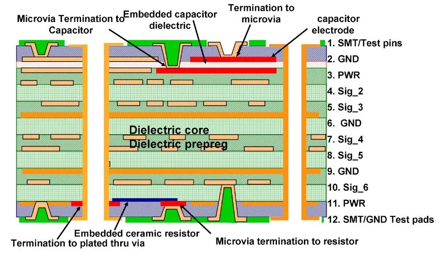
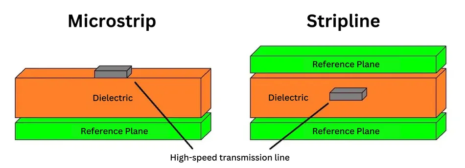
Characteristic impedance in PCBs arises from the interaction between conductive traces and surrounding dielectrics, primarily determined by trace width, thickness, dielectric height, and material properties like dielectric constant. For microstrip configurations, common in outer layers, the exposed trace couples with air and substrate, yielding higher impedance compared to stripline structures fully embedded in dielectric. Trace impedance calculations account for these geometries, with narrower traces or thicker dielectrics increasing Z0. Factory engineers use field solvers during stackup development to predict values, factoring in copper roughness and plating variations that subtly alter effective permittivity at high frequencies.
Stackup impedance emerges from multilayer interactions, where core and prepreg thicknesses define separation between signal and reference planes. Variations in resin content or glass transition temperature can shift dielectric constants, impacting impedance by several ohms. IPC-2141A provides detailed design guides for high-speed controlled impedance circuit boards, emphasizing the need for symmetric stackups to avoid skew. Skin effect at frequencies above 1 GHz confines currents to trace surfaces, further complicating impedance stability without precise manufacturing controls.
Differential trace impedance requires balanced spacing and length matching between pair members, critical for high-speed serial links. Factory lamination processes must minimize voids that alter local capacitance, ensuring pair impedance stays within tolerance.
Material Selection for High-Frequency Impedance Control
Material choice directly determines achievable impedance stability and insertion loss. Low-Dk, low-Df laminates minimize capacitance variations and dielectric losses at GHz frequencies. The table below compares popular options (values at ~10 GHz unless noted):
| Material | Dk (Process) | Df | Key Advantages | Typical Applications |
|---|---|---|---|---|
| Standard FR-4 | 4.0–4.7 | 0.015–0.020 | Low cost, easy processing | General digital (<5 GHz) |
| Rogers RO4003C | 3.38 ± 0.05 | 0.0027 | Excellent RF stability, low cost | Microwave, 5G antennas |
| Rogers RO4350B | 3.48 ± 0.05 | 0.0037 | UL 94V-0, lead-free compatible | High-reliability radar, RF |
| Panasonic Megtron 6 | 3.4–3.6 | ~0.004 | Low loss for >25 Gbps, good thermal | High-speed networking |
| Isola I-Tera MT40 | 3.38–3.75 | 0.0028–0.0035 | Cost-effective PTFE alternative | Servers, 5G infrastructure |
Manufacturing Processes for Controlled Impedance PCBs
Achieving controlled impedance starts with material selection, favoring low-loss dielectrics with stable dielectric constants across frequency ranges. During lamination, precise control of press cycles prevents thickness variations that directly affect stackup impedance. Etching processes demand tight tolerances on trace width and spacing, often held to plus or minus 10 percent to meet impedance specs. Plating uniformity on inner layers influences surface roughness, which at high frequencies contributes to insertion loss alongside impedance deviations. Achieving consistent dielectric height is critical—see our detailed high-speed PCB stackup design mastering impedance control and signal loss for layer sequencing best practices.
Impedance control extends to drilling and via design, where stubs can introduce discontinuities unless back-drilled or filled appropriately. IPC-6012F outlines qualification requirements for rigid printed boards, including dimensional stability critical for impedance performance. Factories implement real-time monitoring of etch rates and develop etch factors tailored to copper weights used in high-frequency designs.
Post-etch inspection verifies geometry before final assembly, with adjustments made to artwork if initial coupons show deviations.
Fine-line etching tolerances become even more critical when routing high-speed signals—review proven techniques in high speed PCB routing achieving impedance control for signal integrity.
Best Practices for Impedance Control in Production
Designers collaborate with manufacturers early to define impedance tolerances, typically plus or minus 10 percent for standard high-frequency boards and tighter for RF applications. Stackup drawings should specify target impedances, test coupon locations, and reference planes clearly. Factories recommend dedicated impedance test traces on panel borders, enabling verification without risking flight boards. Material qualification ensures batch-to-batch consistency, avoiding surprises from dielectric variations.
IPC-2221A serves as a generic standard for printed board design, guiding conductor sizing and layer sequencing for optimal impedance. During fabrication, sequential lamination for complex stackups maintains plane-to-trace distances. Engineers benefit from specifying coplanar waveguide structures where ground pours shield traces, stabilizing impedance in dense layouts.
Impedance Testing Methods and Verification
Impedance testing confirms that manufactured controlled impedance PCBs meet specifications through non-destructive techniques. Time Domain Reflectometry (TDR) sends step pulses along traces, measuring reflections to plot impedance profiles with resolution down to millimeters. Vector Network Analyzers (VNA) provide frequency-domain S-parameter data, extracting effective dielectric constants and losses alongside impedance.
Factories perform 100 percent coupon testing per panel, correlating results to production parameters for process control. IPC-2141A recommends calibration standards like air lines for TDR accuracy, ensuring traceability. Post-solder testing verifies if reflow alters stackup impedance due to material flow.
Advanced cross-section analysis validates stackup dimensions, bridging electrical and physical measurements.
Troubleshooting Common Impedance Control Challenges
Deviations in trace impedance often stem from etch undercut, where isotropic etching narrows traces beyond specs. Factories mitigate this by optimizing developer chemistry and exposure times, targeting etch factors around 2 to 3. Dielectric thickness variations from uneven flow during lamination cause capacitance shifts, addressed through improved prepreg control and vacuum pressing.
Vias introduce impedance bumps if antipad sizes mismatch; enlarging clearances or using blind vias resolves this. High-frequency losses from rough copper demand low-profile foils, verified via surface profilometry. When coupons pass but flight traces fail, panel warpage or registration errors are suspects, corrected by enhanced baking and alignment systems.
Real-World Case Study: 77 GHz Radar Module
A major automotive supplier producing 77 GHz radar modules for ADAS faced impedance variation of ±12% across temperature swings, resulting in 12% field failure rates and ranging errors exceeding design targets. Switching to Rogers RO4350B laminates, implementing symmetric 8-layer stackups, and enforcing ±5% tolerance with 100% TDR coupon testing plus SPC monitoring delivered dramatic results. Impedance stability improved to under 5% variation from –40°C to +125°C, first-pass yield rose to 98%, and field returns dropped below 1%. Target recognition accuracy reached 98.7% even in heavy rain, directly enhancing vehicle safety while cutting monthly rework costs by tens of thousands. The optimized process proved repeatable across multiple fabrication partners.
Future Trends in High-Frequency Impedance Control
By 2025–2030, AI-driven tools will auto-optimize stackups and routing for target Z0 Z_0 Z0 while predicting manufacturing variation, slashing design cycles by 30%. Glass-core substrates with ultra-low Dk and near-zero CTE mismatch to silicon will enable 224 Gbps+ signaling and 100 GHz+ 6G front-ends with minimal loss. Additive manufacturing (3D-printed dielectrics and conductors) will allow custom transmission-line geometries impossible with subtractive etching. Antenna-in-package (AiP) integration will embed controlled-impedance transitions directly with RFICs, eliminating board-level discontinuities. Closed-loop manufacturing with inline TDR feedback will achieve near-zero-defect “lights-out” production for high-frequency PCBs.
Conclusion
Mastering impedance control in high-frequency PCB manufacturing integrates design foresight, process discipline, and rigorous testing. Controlled impedance PCBs deliver superior signal integrity when trace impedance, stackup impedance, and manufacturing tolerances align. Electric engineers gain reliability by leveraging standards like IPC-2141A and IPC-6012F throughout the supply chain. Factories that prioritize these elements reduce iterations, accelerate time-to-market, and support demanding applications. Consistent application of best practices ensures performance from prototype to production.
FAQs
Q1: What factors most influence trace impedance in controlled impedance PCBs?
A1: Trace impedance depends on width, thickness, dielectric height, and material dielectric constant. In manufacturing, etch tolerances and lamination uniformity play key roles. Stackup design further refines these by controlling reference plane proximity. Engineers specify these early to achieve targets like 50 ohms single-ended.
Q2: How does stackup impedance affect high-frequency signal performance?
A2: Stackup impedance determines capacitance between layers, directly impacting characteristic impedance. Asymmetric builds cause variations, leading to reflections. Factories use symmetric cores and prepregs per IPC guidelines for stability. Proper stackup ensures minimal loss and consistent propagation delay.
Q3: What is the standard method for impedance testing in PCB production?
A3: TDR and VNA are primary for impedance testing, measuring reflections and S-parameters respectively. Test coupons on panels verify trace impedance without board damage. Tolerances of plus or minus 10 percent are common. Factories calibrate equipment regularly for accuracy.
Q4: Why is impedance control critical for high-frequency PCBs?
A4: Impedance control prevents mismatches causing signal distortion at GHz frequencies. It maintains waveform integrity in RF and high-speed digital circuits. Manufacturing adherence to specs avoids costly respins. Standards like IPC-6012F enforce performance criteria.
References
IPC-2141A — Design Guide for High-Speed Controlled Impedance Circuit Boards. IPC, 2004
IPC-6012F — Qualification and Performance Specification for Rigid Printed Boards. IPC, 2023
IPC-2221A — Generic Standard on Printed Board Design. IPC, 2003