Introduction
The FR-1 PCB manufacturing process represents a cornerstone of cost-effective electronics production for simple, single-sided circuit boards. Engineers often select FR-1 for applications where high volume and low complexity align with budget constraints. This guide breaks down the PCB fabrication steps from raw material preparation to final quality checks, emphasizing factory-floor precision. Understanding these stages ensures reliable outcomes in production runs. Factory insights reveal that mastering FR-1 processes minimizes scrap rates and optimizes throughput. By following standard-aligned procedures, teams achieve consistent performance in consumer and industrial products.
What Is FR-1 PCB Material?
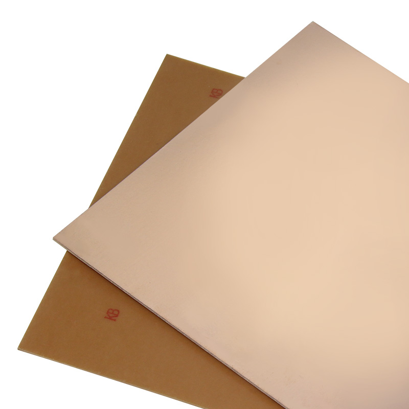
FR-1 consists of cellulose paper impregnated with phenolic resin, forming a flame-retardant substrate clad with copper foil on one side. This paper-based laminate provides mechanical stability while keeping costs low compared to glass-epoxy alternatives. The material meets specifications in IPC-4101 for base materials used in rigid printed boards. Its glass transition temperature sits around 130 degrees Celsius, suitable for low-power operations. Copper thickness typically measures 1 ounce per square foot, enabling straightforward etching for basic traces. Engineers value FR-1 for its punchability and light weight in single-layer designs.
The phenolic resin imparts self-extinguishing properties, aligning with safety needs in enclosed electronics. Moisture absorption remains a consideration, prompting storage protocols in humid environments. Dimensional stability holds during standard soldering profiles below 245 degrees Celsius. FR-1 supports surface-mount or simple through-hole components without plated vias. Factory experience shows it excels in high-volume punching over drilling for certain features. Overall, its composition drives economy without sacrificing basic functionality.
Why FR-1 PCBs Matter in Manufacturing
FR-1 PCBs fill a critical niche for low-density circuits in consumer devices like remote controls and power adapters. Cost savings of 40 to 60 percent over advanced materials make it indispensable for mass production. Single-sided construction simplifies the PCB fabrication steps, reducing equipment needs and cycle times. In factories, FR-1 enables rapid prototyping and scaling for educational kits or novelty items. Its compliance with IPC-A-600 acceptability criteria ensures visual and electrical reliability. Engineers benefit from predictable behavior in wave soldering processes.
Demand persists in regions prioritizing affordability over high-speed performance. FR-1 avoids the dust hazards of fiberglass machining, enhancing worker safety on the floor. Applications in control panels and LED fixtures leverage its trace widths down to 0.2 millimeters. Limitations like poor multilayer support steer designs toward appropriate uses. Factory data indicates scrap rates around 3 percent with proper handling. Ultimately, FR-1 sustains viable production for non-critical electronics. Learn how this material compares with FR-4 and other laminates in our detailed FR1 vs FR2 vs FR3 vs FR4 guide.
The FR-1 PCB Manufacturing Process: Step-by-Step Guide
1. Material Preparation and Lamination
Production begins with selecting high-quality cellulose paper as the core substrate. This paper undergoes impregnation with phenol-formaldehyde resin in controlled baths to achieve uniform saturation. The resin-cured sheets then bond to copper foil under heat and pressure in a hot press, forming rigid panels. Factory presses maintain temperatures around 150 to 180 degrees Celsius for optimal adhesion. Resulting laminates exhibit the characteristic brown hue and flame-retardant traits. Panels cure fully before further processing to prevent delamination. Always verify thermal limits before final design—read our full analysis of FR-1 PCB temperature limits.
2. Panel Sizing and Cutting
Laminated sheets cut into workable panel sizes using shear or guillotine tools. Dimensions match customer panelization layouts, typically 18 by 24 inches for efficiency. Edge beveling prevents burrs during handling. Factories inspect for copper adhesion and thickness uniformity at this stage. Clean cuts minimize waste in downstream steps. Panels stack and store in climate-controlled areas to limit moisture uptake.
3. Drilling FR-1 PCB Holes
Drilling FR-1 PCB panels employs CNC machines with carbide bits starting at 0.6 millimeter diameters. The paper core yields cleanly, avoiding fiberglass dust but requiring vacuum extraction for resin particles. Holes align precisely to fiducials using optical registration. Feed rates adjust to 1 to 2 meters per minute, balancing speed and hole quality. Deburring follows with chemical or mechanical methods to clear debris. This step prepares sites for component leads without plating needs.
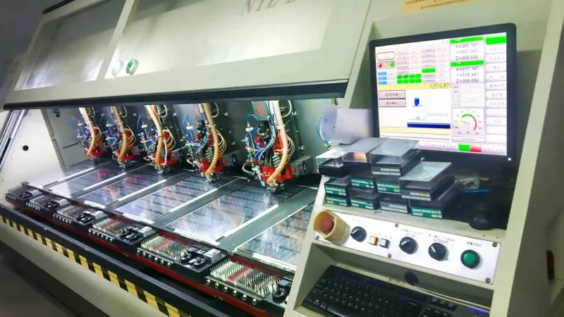
Multi-spindle heads process arrays efficiently, hitting tolerances of plus or minus 0.1 millimeter. Factories program stacks up to 10 panels with entry-exit materials for straightness. Visual checks confirm no breakout or smear. Drilling FR-1 PCB demands bit sharpening every 500 panels to sustain edge quality.
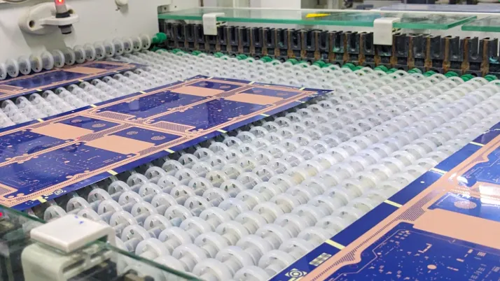
4. Photoresist Application and Imaging
Dry film photoresist laminates onto the copper side via hot roll at 90 to 110 degrees Celsius. Film thickness matches trace requirements, typically 1.5 mils. Panels expose under UV light through photoplotter-generated artwork, hardening resist in circuit patterns. Development in sodium carbonate solution removes unexposed areas, revealing etch areas. Alignment ensures overlay accuracy within 0.075 millimeters. Factory cleanrooms control dust to prevent imaging defects.
5. FR-1 PCB Etching Techniques
FR-1 PCB etching techniques use ferric chloride solutions in conveyorized spray systems for uniform copper removal. Etchants operate at 45 to 55 degrees Celsius with pH monitoring for consistent undercutting. Conveyor speed controls dwell time to 5 to 15 minutes, preserving 0.2 millimeter minimum traces. Rinse cascades follow to halt reactions and clear residues. Factories regenerate etchant to cut costs and waste. Post-etch inspection verifies line widths via automated optical systems.
Inline etching favors FR-1 due to thin copper, minimizing lateral etch. Bubble agitation enhances mass transfer for sidewall control. Waste treatment neutralizes spent solutions per environmental rules. Etching defines the circuit pattern critical to functionality.
6. Resist Stripping and Cleaning
Sodium hydroxide baths strip remaining photoresist at 50 degrees Celsius. High-pressure sprays remove residues without damaging traces. Micro-etch dips refine copper surfaces for solderability. Drying ovens evaporate moisture completely. Panels undergo oxide prevention if delayed before finishing. Cleanliness tests confirm ionic contamination below 2 micrograms per square centimeter equivalent sodium chloride.
7. Final Fabrication and Finishing
Solder mask applies optionally via screen print or liquid photoimageable film for basic protection. Curing bakes at 150 degrees Celsius solidify the mask. Silkscreen legend prints component IDs on the bare side. Routing or V-scoring separates individual boards from panels using carbide end mills. Beveling edges aids insertion. Factories fixture boards for flying probe testing continuity and shorts.
8. FR-1 PCB Quality Control
FR-1 PCB quality control spans visual, dimensional, and electrical verification per IPC-6012 guidelines. Automated optical inspection scans for opens, shorts, and anomalies. Microsectioning samples assesses drill quality and copper adhesion. Solderability tests dip samples in fluxed solder pots. Final packaging uses vacuum bags to block humidity. Traceability logs track panels from laminate to shipment.
Best Practices for FR-1 PCB Fabrication
Maintain panel flatness below 0.75 percent to avoid imaging misalignment. Use entry boards during drilling FR-1 PCB to control breakout. Optimize etchant specific gravity at 1.3 to 1.4 for clean etching. Store laminates at 50 percent relative humidity maximum. Implement statistical process control for etch depth uniformity. Train operators on IPC-A-600 Class 2 criteria for acceptance.
Select resist compatible with phenolic outgassing. Fixture panels rigidly for exposure. Regenerate etchants weekly to sustain performance. Perform 100 percent electrical test at 20 volts. Document deviations for continuous improvement. For hands-on projects, see our guide on transitioning from breadboards to FR-1 PCB circuit construction.
Common Challenges and Troubleshooting
Moisture absorption swells panels, causing drill wander; bake panels at 105 degrees Celsius for two hours pre-process. Etch undercut exceeds specs if conveyor slows; calibrate speeds daily. Poor resist adhesion from oils leads to under-etch; enhance panel cleaning. Warpage post-lamination corrects with symmetric scoring. Component hole misalignment traces to drill registration; verify fiducials. Factory root-cause analysis resolves 90 percent of issues via these steps.
Conclusion
Mastering the FR-1 PCB manufacturing process delivers economical, reliable boards for targeted applications. Each PCB fabrication step, from lamination to FR-1 PCB quality control, demands precision aligned with industry standards. Engineers gain efficiency by anticipating material traits like punchability and temperature limits. Factories thrive on best practices reducing defects and costs. This guide equips teams for successful production runs.
FAQs
Q1: What are the key PCB fabrication steps for FR-1 boards?
A1: The FR-1 PCB manufacturing process starts with paper resin impregnation and copper lamination, followed by cutting, drilling FR-1 PCB holes, photoresist imaging, etching, stripping, finishing, and testing. Factories prioritize clean drilling and controlled etching to maintain trace integrity. Single-sided nature simplifies flow compared to multilayer boards. Standards like IPC-4101 guide material selection.
Q2: How do FR-1 PCB etching techniques differ from other materials?
A2: FR-1 PCB etching techniques rely on ferric chloride sprays due to thin single-side copper, achieving clean removal in 5 to 15 minutes. Paper core stability aids uniform etching without plating concerns. Factories monitor temperature and agitation for minimal undercut on 0.2 millimeter traces. Post-etch cleaning prevents residue issues.
Q3: What quality checks are essential in drilling FR-1 PCB?
A3: Drilling FR-1 PCB requires verifying hole diameters from 0.6 millimeters, alignment to fiducials, and absence of smear or breakout. CNC programming ensures straightness with vacuum debris removal. Microsection analysis confirms wall quality. IPC-A-600 criteria classify acceptability for production.
Q4: Why is FR-1 PCB quality control critical for single-sided boards?
A4: FR-1 PCB quality control prevents moisture-induced failures and etch defects through visual, electrical, and solderability tests. Flying probe verifies continuity without fixtures. Dimensional checks maintain tolerances. Factory protocols per IPC-6012 ensure reliability in cost-sensitive applications.
References
IPC-4101E — Specification for Base Materials for Rigid and Multilayer Printed Boards. IPC, 2010
IPC-A-600K — Acceptability of Printed Boards. IPC, 2020
IPC-6012E — Qualification and Performance Specification for Rigid Printed Boards. IPC, 2017
IPC-2221B — Generic Standard on Printed Board Design. IPC, 2012


