Introduction
Electronic hobbyists often push the limits of their projects into harsh environments, such as automotive engines, industrial furnaces, or even custom 3D printers, where standard PCBs fail under extreme heat. A ceramic PCB temperature sensor circuit stands out as a reliable solution for these high-temperature sensor applications, offering durability where organic substrates like FR-4 cannot compete. Ceramic PCBs excel due to their superior thermal conductivity and stability at temperatures exceeding 200 degrees Celsius, making them ideal for sensor circuit design in demanding sensor projects. This article guides you through building a high-temperature sensor on a ceramic PCB, from principles to practical assembly, tailored for hands-on enthusiasts. By the end, you’ll understand how to create a robust ceramic PCB project that measures temperatures accurately in real-world scenarios. Let’s dive into the fundamentals and step-by-step process.

What Is a Ceramic PCB and Why It Matters for High-Temperature Sensors
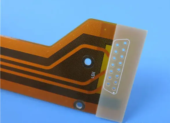
Ceramic PCBs use inorganic substrates like alumina or aluminum nitride, which provide exceptional mechanical strength and electrical insulation even at elevated temperatures. Unlike traditional laminates, these boards resist thermal shock and maintain dimensional stability, crucial for high-temperature sensor circuits that operate continuously in hot zones. For electronic hobbyists, this means your sensor projects can handle environments up to 850 degrees Celsius without warping or delaminating, extending the lifespan of devices like exhaust gas analyzers or kiln monitors. The high thermal conductivity, often over 20 W/mK, efficiently dissipates heat from sensitive components, preventing false readings in ceramic PCB temperature sensor setups. Industry relevance grows as hobbyists experiment with IoT-enabled monitoring in aerospace models or renewable energy prototypes, where reliability trumps cost. Choosing ceramic elevates your ceramic PCB project from prototype to production-ready. Compare ceramic substrates with other high-performance materials in our Ceramic PCB vs. FR-4: Choosing the Right Material for Your High-Frequency Design.
This material choice aligns with performance needs in sensor circuit design, where signal integrity must persist amid thermal cycling. Hobbyists benefit from reduced noise in analog signals, as ceramics minimize CTE mismatch with high-temp components like thermocouples.
Technical Principles Behind High-Temperature Sensor Circuits on Ceramic PCBs
High-temperature sensors, such as Type K thermocouples, generate voltage based on the Seebeck effect, producing millivolts proportional to temperature differences between hot and cold junctions. In a ceramic PCB temperature sensor, the circuit amplifies this signal using operational amplifiers rated for 175 degrees Celsius or higher, ensuring precision across wide ranges. Ceramic substrates support thick-film resistors and conductors fired at high temperatures, forming stable networks that resist oxidation and drift. The low dielectric constant of ceramics reduces parasitic capacitance, vital for accurate sensor circuit design in noisy environments. Thermal management principles dictate trace widths wider than standard to handle heat flux, preventing hotspots that could skew measurements.
Power supply regulation becomes key, often using linear regulators with ceramic capacitors for stability under thermal stress. Ground planes on both sides enhance shielding, while vias plated with high-melt alloys maintain connectivity. Adhering to IPC-A-600 guidelines for acceptability ensures surface finishes withstand firing processes without defects.
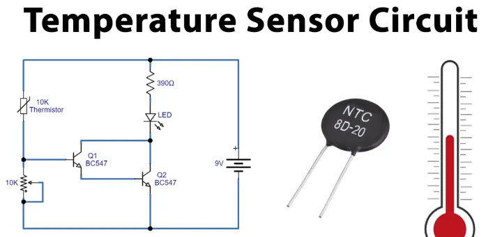
Signal conditioning involves cold junction compensation, typically via a precision reference IC mounted near the cold junction on the ceramic PCB. This setup corrects for ambient variations, achieving accuracy within 1 degree Celsius over 1000 degrees Celsius spans.
Practical Solutions and Best Practices for Building Your Ceramic PCB Project
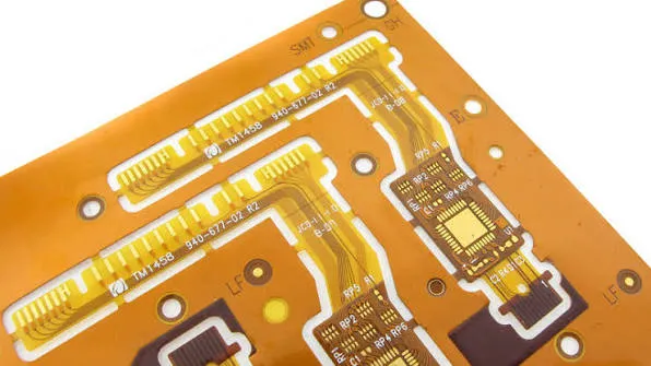
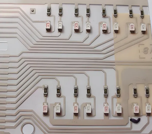
Start with schematic capture, focusing on a thermocouple front-end followed by a gain stage and output buffer for ADC interfacing. Select components with matching CTE to the ceramic base, such as wire-bondable chips or surface-mount passives rated for 250 degrees Celsius. For hobbyists, design traces with 0.5 mm minimum width for 1A currents, using software to simulate thermal profiles and verify voltage drops. Layer stackup typically includes a single or double-sided ceramic with screen-printed silver or gold conductors, fired to form hermetic seals.
Fabrication involves photolithography for fine features down to 50 microns, followed by high-temperature sintering around 850 degrees Celsius. Order prototypes with gold plating for wire bonding if embedding sensors directly. Assembly uses high-melt solder like 96.5Sn-3Ag-0.5Cu, applied via reflow profiles per J-STD-020 to avoid voids. For sensor integration tips in extreme environments, see Integrating Sensors on Navigation System PCBs: A Design Guide.
Testing protocols include thermal cycling from -40 to 300 degrees Celsius, checking for opens or resistance shifts per IPC-TM-650 methods. Calibrate the high-temperature sensor against a reference thermometer in an oven, adjusting gain trimpots for linearity. Encapsulate the board in high-temp epoxy for vibration resistance in mobile sensor projects.
Enclose the circuit in a metal housing with thermal vias to the ambient for cold junction stability. Power it from a 5V regulator with decoupling caps placed 1 mm from pins.
Troubleshooting Common Issues in High-Temperature Sensor Circuits
Hobbyists often encounter offset drifts in ceramic PCB temperature sensors due to thermocouple junction inconsistencies. Verify polarity and use extension wires of the same type to minimize errors. If amplification saturates, probe stages with a high-impedance meter to isolate gain issues.
Warpage after firing signals substrate thickness mismatches; select 0.635 mm alumina for balance. Signal noise points to poor grounding; add stitching vias around the sensor area.
Component failures stem from CTE mismatches; test solder joints post 100 cycles. Use IPC-A-600 inspection criteria for pad adhesion before full deployment.
Firmware glitches in microcontroller interfaces require averaging multiple readings to filter transients. Learn more about high-temperature material selection in Smart Grid PCB Materials: Choosing the Right Substrate for Performance.
Conclusion
Building a high-temperature sensor circuit on a ceramic PCB empowers electronic hobbyists to tackle extreme environments with confidence, leveraging the material’s thermal prowess for precise sensor circuit design. From understanding thermocouple principles to mastering assembly best practices, this ceramic PCB project delivers robust performance in sensor projects. Key takeaways include prioritizing CTE-matched components, rigorous thermal testing, and standards-compliant processes for longevity. Experiment with variations like multi-channel arrays for advanced monitoring. Your next high-temperature sensor will outperform off-the-shelf options, opening doors to innovative applications.
FAQs
QX: What makes a ceramic PCB ideal for a high-temperature sensor circuit?
AX: Ceramic PCBs offer high thermal conductivity and low CTE, allowing them to operate reliably above 200 degrees Celsius without degradation. This suits ceramic PCB temperature sensor designs where FR-4 would warp or lose integrity. Hobbyists appreciate the stability for sensor projects in ovens or engines, ensuring accurate readings over time. Follow J-STD-020 reflow guidelines during assembly for best results.
QX: How do I design a basic high-temperature sensor on a ceramic PCB?
AX: Start with a Type K thermocouple connected to an op-amp for signal amplification, using thick-film resistors on the ceramic substrate. Simulate the circuit for gain and offset, then layout with wide traces for heat dissipation. This sensor circuit design handles 1000 degrees Celsius spans effectively. Test in stages to verify linearity in your ceramic PCB project.
QX: What are common challenges in ceramic PCB temperature sensor projects?
AX: Thermal expansion mismatches can crack solder joints, so select high-temp alloys and cycle-test per IPC-TM-650. Noise from EMI requires ground planes and shielding. For hobbyists, calibration against standards resolves drift in high-temperature sensors. Proper encapsulation boosts durability in real-world sensor projects.
QX: Can electronic hobbyists prototype a high-temperature sensor circuit affordably?
AX: Yes, by designing simple schematics and using standard ceramic substrates like alumina. Focus on fewer layers to control costs while maintaining performance. Assembly with manual soldering works for prototypes, evolving into reflow for production. This approach makes ceramic PCB projects accessible for sensor circuit design enthusiasts.
References
IPC-A-600K — Acceptability of Printed Boards. IPC, 2020
J-STD-020E — Moisture/Reflow Sensitivity Classification. JEDEC, 2014
IPC-TM-650 — Test Methods Manual. IPC, 2022