
lead-free-pcb-design
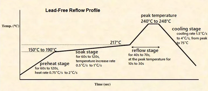
Lead-free PCB design has become a cornerstone of modern electronics manufacturing, driven by global regulations such as the Restriction of Hazardous Substances (RoHS) directive. This approach eliminates the use of lead in solder alloys and components, promoting safer, more environmentally friendly products while ensuring compliance with international standards. For engineers, designers, and manufacturers searching for guidance on lead-free PCB design, this tag compiles essential resources that address the transition from traditional lead-based methods. You'll find in-depth discussions on selecting compatible materials like tin-silver-copper (SAC) alloys, optimizing reflow soldering profiles to prevent defects such as tombstoning or voids, and implementing robust testing protocols to verify reliability. Understanding the practical applications of lead-free PCB design is crucial for achieving high-performance circuits without compromising durability. Key best practices include designing for higher thermal stresses, as lead-free solders often require elevated temperatures during assembly, which can impact component longevity. Articles under this tag explore strategies for mitigating common challenges, such as intermetallic compound formation and whisker growth, through advanced techniques like conformal coating and precise via filling. Whether you're developing consumer electronics, automotive systems, or medical devices, these insights provide actionable steps to enhance board integrity and reduce failure rates in lead-free environments. By delving into the content here, you can gain a comprehensive view of evolving industry standards and innovative solutions. Related articles offer detailed case studies and tutorials that build on these fundamentals, helping you apply lead-free principles effectively in your projects. This collection serves as a valuable reference for staying ahead in sustainable PCB development.
Video Guide
No videos found for this tag.
Technical Articles
Get in Touch
Send Message
- Products & Service
- Company
- About AIVON
- Contact
- News
- Blog
- Certification
-


- Payment
-


2026 AIVON.COM All Rights Reserved