PCB Fault Finding
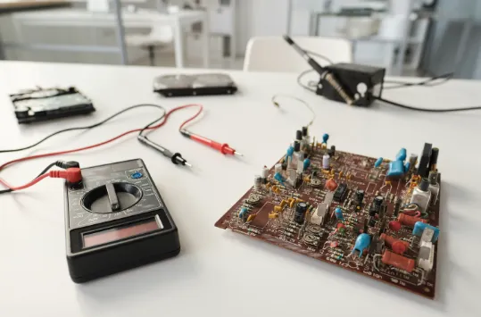
PCB Fault Finding is an essential discipline in electronics engineering and repair, focusing on the systematic identification and resolution of issues within printed circuit boards (PCBs). Whether you are a professional technician troubleshooting complex assemblies or a hobbyist diagnosing failures in custom projects, understanding common faults such as short circuits, open traces, component failures, or soldering defects can significantly reduce downtime and repair costs. This tag aggregates in-depth articles that delve into proven methodologies, from visual inspections and multimeter testing to advanced techniques like thermal imaging and oscilloscope analysis, ensuring you have the tools to pinpoint problems efficiently. For those arriving via search queries related to PCB Fault Finding, our content emphasizes practical applications tailored to real-world scenarios. Learn best practices for isolating faults in multilayer boards, interpreting schematic diagrams, and using non-destructive testing methods to avoid further damage. We cover step-by-step guides on employing tools like boundary scan testing or in-circuit emulators, alongside tips for preventing common pitfalls such as electrostatic discharge or thermal stress. These insights not only help in immediate troubleshooting but also in designing more robust PCBs for future projects, drawing from industry standards and case studies. As you navigate this tag, you will find articles that build on these foundations, offering detailed walkthroughs and expert advice to enhance your diagnostic skills. This resource serves as a comprehensive hub for refining your approach to PCB maintenance, ultimately leading to more reliable electronic systems.
Video Guide
No videos found for this tag.
Technical Articles
Get in Touch
Send Message
- Products & Service
- Company
- About AIVON
- Contact
- News
- Blog
- Certification
-


- Payment
-


2026 AIVON.COM All Rights Reserved