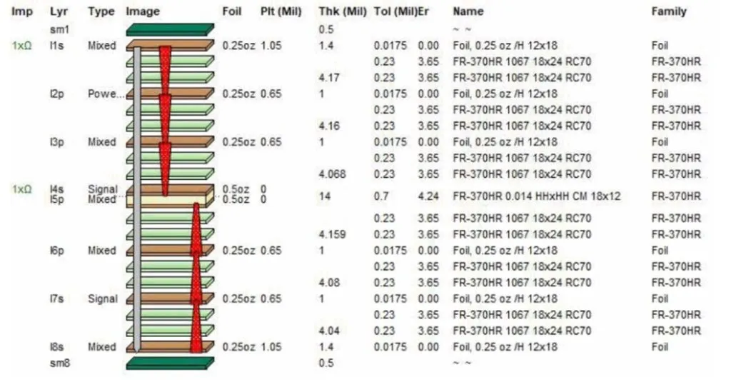
Sequential Build-Up
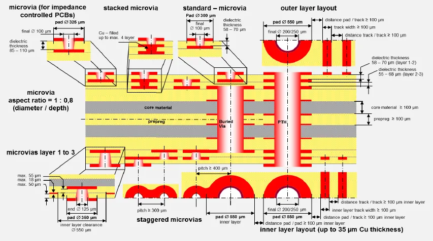
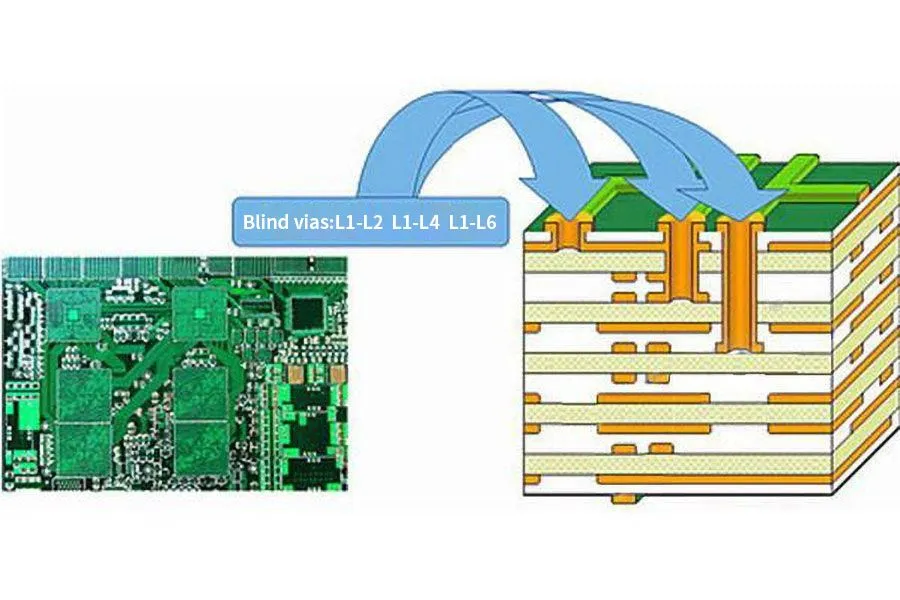
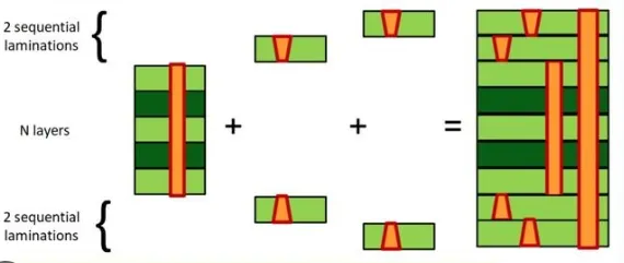
Sequential build-up is a key manufacturing technique in printed circuit board (PCB) design, particularly for creating high-density interconnect (HDI) boards that support complex electronic systems. This method involves layering dielectric materials and conductive traces sequentially, often incorporating microvias, buried vias, and blind vias to achieve compact, multilayer structures without the limitations of traditional lamination processes. By building up layers one at a time, engineers can optimize signal integrity, reduce crosstalk, and enhance thermal management, making it ideal for applications in smartphones, medical devices, automotive electronics, and high-speed computing. For professionals and hobbyists searching for information on sequential build-up, understanding its practical applications can streamline design workflows and improve product reliability. This approach allows for finer pitch components and higher routing density, which is crucial when space constraints demand innovative solutions. Best practices include selecting appropriate dielectric materials to minimize signal loss, ensuring precise via filling to prevent defects, and conducting thorough simulations to validate layer stacking before fabrication. These steps help avoid common pitfalls such as delamination or impedance mismatches, ultimately leading to cost-effective production and faster time-to-market. Readers interested in diving deeper into sequential build-up techniques will find valuable insights in our collection of articles, covering topics from material selection to advanced HDI fabrication methods. Whether you are troubleshooting a design issue or exploring new PCB technologies, these resources provide the technical depth needed to apply this method effectively in your projects.
Video Guide
No videos found for this tag.
Technical Articles
Get in Touch
Send Message
- Products & Service
- Company
- About AIVON
- Contact
- News
- Blog
- Certification
-


- Payment
-


2026 AIVON.COM All Rights Reserved