Introduction
Flexible electronics represent a transformative shift in circuit design, driven by the demand for devices that conform to irregular shapes and endure mechanical stress. Organic substrate PCBs, particularly those using polyimide films, enable this evolution by providing the necessary flexibility without sacrificing electrical performance. These flexible PCB organic substrates combine lightweight construction with high reliability, making them ideal for applications where traditional rigid boards fall short. Engineers increasingly turn to bendable PCB design to integrate circuits into wearables, medical implants, and aerospace components, reducing overall system weight and volume. As industries push for miniaturization and durability, understanding the principles behind organic substrate PCB applications becomes essential for optimizing performance. This article explores the materials, design strategies, and best practices that allow these boards to bend the rules of conventional PCB engineering.
What Are Organic Substrate PCBs for Flexible Electronics?
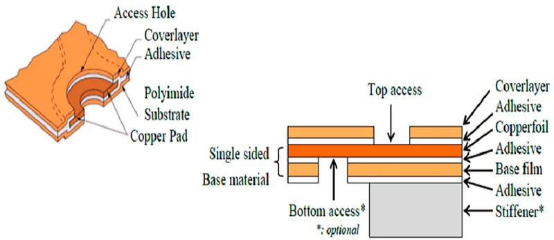
Organic substrate PCBs rely on polymer-based materials as the core dielectric, distinguishing them from rigid inorganic alternatives like ceramics. In flexible variants, polyimide serves as the primary organic substrate due to its excellent thermal stability and mechanical flexibility. These boards consist of thin copper foils laminated onto the substrate, often without adhesives to enhance bend endurance. Flexible PCB organic substrates come in single-sided, double-sided, or multilayer configurations, each tailored to specific flex requirements. The key advantage lies in their ability to withstand repeated bending, folding, or twisting while maintaining signal integrity.
These boards matter because they address critical limitations in rigid PCB designs, such as bulkiness and inflexibility in compact spaces. Lightweight PCB solutions using organic substrates reduce assembly weight by up to significant margins compared to glass-epoxy laminates, vital for portable and aerospace applications. In consumer electronics, they enable seamless integration into curved displays or foldable devices. For electric engineers, the relevance stems from improved reliability in dynamic environments, where vibration and movement are constant. Compliance with standards like IPC-6013 ensures qualification for high-performance uses. Overall, organic substrate PCBs expand design possibilities, fostering innovation in organic substrate PCB applications.
Technical Principles Behind Organic Substrate PCBs
The foundation of flexible PCB organic substrates rests on the intrinsic properties of materials like polyimide, which exhibits a high glass transition temperature and low coefficient of thermal expansion. This polymer maintains integrity across wide temperature ranges, resisting delamination during soldering or operation. Copper conductors, typically rolled annealed for ductility, bond directly to the substrate in adhesiveless constructions, minimizing peel strength issues under flex. The dielectric's thin profile, often in the range of common thicknesses, allows tight radii without fracturing traces. Electrical properties include low dielectric constant for signal speed and controlled impedance matching.
Bending mechanics involve strain distribution across layers, with the neutral axis positioned to reduce copper fatigue. In bendable PCB design, dynamic flexing induces cyclic stress, demanding materials with high fatigue life. Polyimide PCBs excel here, supporting millions of cycles in qualified tests. Multilayer stacks incorporate coverlays for protection, while rigid-flex hybrids blend organic flex tails with stiffeners. Thermal management relies on the substrate's heat dissipation, preventing hotspots in high-density routing. Factory processes emphasize lamination under vacuum to avoid voids, ensuring void-free interfaces per industry norms.
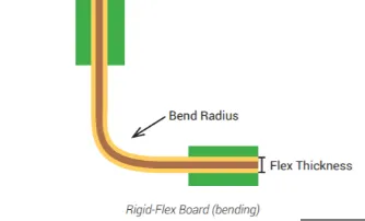
IPC-2223 provides guidelines for calculating allowable bend radii based on layer count and copper thickness, factoring in modulus of elasticity. For static applications, ratios scale with board thickness to prevent cracking. These principles guide engineers in predicting lifespan through finite element analysis during prototyping.
Best Practices for Bendable PCB Design with Organic Substrates
Effective bendable flexible PCB design starts with defining flex and rigid zones clearly in the stackup, isolating high-stress areas from components. Traces in bend regions should follow curved paths with generous fillets, avoiding 90-degree angles that concentrate strain. Minimum spacing increases in flex tails to accommodate elongation, typically wider than rigid sections. Polyimide PCB selection prioritizes adhesiveless laminates for repeated flexing, enhancing copper-substrate adhesion. Stiffeners, such as polyimide or FR4 tabs, reinforce mounting areas without compromising overall flexibility.
Manufacturing alignment with IPC-6013 involves precise etching control to maintain trace integrity post-flex. Coverlay application requires alignment tolerances to shield conductors uniformly. For lightweight PCB solutions, thinner copper foils pair with minimal substrate layers, balancing conductivity and weight. Solder mask alternatives like photoimageable coverlays reduce added thickness. Testing protocols simulate end-use conditions, including thermal cycling and bend endurance.
Engineers should iterate designs with bend radius simulations, adhering to ratios like those in established guidelines for static or dynamic use. Panelization strategies minimize waste during production, while panel fiducials aid registration. These practices ensure reliable organic substrate PCB applications in production volumes.
Key Applications of Organic Substrate PCBs
Organic substrate PCB applications span sectors demanding conformability and reduced mass. In wearables, flexible PCB organic substrates wrap around body contours for sensors in fitness trackers, enduring daily motion. Medical devices leverage polyimide's biocompatibility for implants and endoscopes, where bendable PCB design navigates tight anatomies. Aerospace employs lightweight PCB solutions in unmanned vehicles, slashing fuel costs through minimized wiring harnesses.
Consumer foldables integrate these boards into hinges, supporting high-resolution displays without bulk. Automotive sensors in curved housings benefit from vibration resistance. Industrial robotics uses them for articulated joints, enhancing precision. Each application exploits the substrates' density advantages, enabling three-dimensional layouts unattainable with rigid boards.
Challenges and Mitigation in Flexible Organic Substrate PCBs
Warpage poses a challenge during lamination or reflow, influenced by CTE mismatches between copper and polyimide. Mitigation includes symmetric stackups and controlled cure cycles in factories. Reliability under humidity requires moisture barriers, as organic materials absorb trace amounts affecting insulation resistance. Dynamic fatigue testing verifies cycle life, guiding material qualification.
Solder joint integrity in flex areas demands low-profile components and underfill for strain relief. Dimensional stability post-flex ensures assembly repeatability. Factory-driven insights emphasize cleanroom handling to prevent contamination on exposed copper.
Conclusion
Organic substrate PCBs redefine flexible electronics through polyimide's robust properties and precise bendable PCB design. From lightweight PCB solutions to diverse applications, they deliver unmatched adaptability. Adhering to standards like IPC-6013 and IPC-2223 ensures performance and manufacturability. Engineers gain freedom to innovate, bending traditional constraints for next-generation devices. Prioritizing these principles yields durable, efficient circuits ready for demanding environments.
FAQs
QX: What materials are used in flexible PCB organic substrates?
AX: Polyimide films dominate as the core organic substrate due to superior flexibility, thermal resistance, and chemical stability. These adhesiveless or adhesive-based laminates support copper conductors for reliable signal transmission. Factory processes qualify them per IPC standards for bend endurance. This choice enables lightweight PCB solutions in compact designs. (52 words)
QX: How does bend radius affect bendable PCB design?
AX: Bend radius determines strain on traces and substrate, with tighter radii risking fatigue in polyimide PCBs. Guidelines recommend multiples of board thickness, scaling by layer count for static or dynamic flex. Curved routing and zone isolation mitigate risks. Proper sizing per IPC-2223 extends lifespan in organic substrate PCB applications. (58 words)
QX: What are common organic substrate PCB applications?
AX: These PCBs suit wearables, medical devices, and aerospace for their conformability and low weight. Flexible PCB organic substrates enable sensors in curved housings or foldable screens. They reduce assembly complexity in robotics and automotive. Durability under motion makes them ideal for dynamic environments. (48 words)
QX: Why choose polyimide for lightweight PCB solutions?
AX: Polyimide offers exceptional strength-to-weight ratio, high flex cycles, and wide temperature tolerance. It outperforms polyester in demanding thermal profiles, supporting fine-pitch routing. This material minimizes overall mass in bendable PCB design, crucial for portables. Factory qualification ensures consistency across volumes. (50 words)
FAQs
Q1: What materials are used in flexible PCB organic substrates?
A1: Polyimide films dominate as the core organic substrate due to superior flexibility, thermal resistance, and chemical stability. These adhesiveless or adhesive-based laminates support copper conductors for reliable signal transmission. Factory processes qualify them per IPC standards for bend endurance. This choice enables lightweight PCB solutions in compact designs.
Q2: How does bend radius affect bendable PCB design?
A2: Bend radius determines strain on traces and substrate, with tighter radii risking fatigue in polyimide PCBs. Guidelines recommend multiples of board thickness, scaling by layer count for static or dynamic flex. Curved routing and zone isolation mitigate risks. Proper sizing per IPC-2223 extends lifespan in organic substrate PCB applications.
Q3: What are common organic substrate PCB applications?
A3: These PCBs suit wearables, medical devices, and aerospace for their conformability and low weight. Flexible PCB organic substrates enable sensors in curved housings or foldable screens. They reduce assembly complexity in robotics and automotive. Durability under motion makes them ideal for dynamic environments.
Q4: Why choose polyimide for lightweight PCB solutions?
A4: Polyimide offers exceptional strength-to-weight ratio, high flex cycles, and wide temperature tolerance. It outperforms polyester in demanding thermal profiles, supporting fine-pitch routing. This material minimizes overall mass in bendable PCB design, crucial for portables. Factory qualification ensures consistency across volumes.
References
IPC-6013E — Qualification and Performance Specification for Flexible/Rigid-Flexible Printed Boards. IPC, 2021
IPC-2223B — Sectional Design Standard for Flexible Printed Boards. IPC, 2017