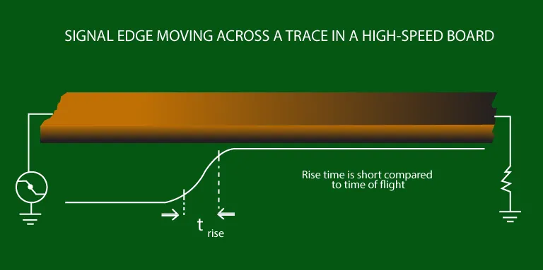
PCB Impedance Control Testing: Ensuring Compliance with Design Specifications
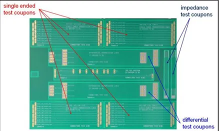
PCB impedance control testing verifies trace performance against design specs using TDR and VNA methods. Review equipment, PCB testing standards like IPC, best practices, troubleshooting, and verification steps for signal integrity and manufacturing compliance in high-speed electronics. Ideal for electrical engineers.