Introduction
Rigid-flex PCBs combine the structural integrity of rigid boards with the adaptability of flexible circuits, enabling compact designs in applications like wearables, medical devices, and aerospace systems. Engineers often encounter rigid-flex PCB design challenges during layout, particularly in bend areas, transitions between rigid and flex sections, and material selection. These issues can lead to failures such as cracking, delamination, or signal integrity problems if not addressed early. Understanding the underlying principles allows designers to create reliable boards that meet performance demands. This article explores practical solutions grounded in engineering best practices, helping electric engineers optimize their rigid-flex PCB design tips for manufacturability and longevity. By focusing on these key areas, teams can reduce iterations and improve yield rates.
What Are Rigid-Flex PCBs and Why Do Design Challenges Matter?
Rigid-flex PCBs integrate rigid substrates, typically for component mounting, with flexible sections that allow bending and folding to fit into tight spaces. This hybrid construction supports higher circuit density and mechanical flexibility compared to all-rigid or all-flex boards. Design challenges arise because the materials and geometries must withstand repeated flexing, thermal cycling, and mechanical stress without compromising electrical performance. Poor bend area design, for instance, can cause copper fatigue, while abrupt transitions concentrate stress leading to tears. Material mismatches exacerbate these problems by causing differential expansion. Addressing rigid-flex PCB design challenges ensures compliance with reliability standards and extends product lifespan in demanding environments.
In the PCB industry, these challenges impact yield, cost, and time-to-market. Engineers must balance electrical, mechanical, and thermal requirements from the schematic stage through fabrication. Ignoring them results in common failures like trace fractures or interlayer separation. Proactive design incorporating rigid-flex PCB troubleshooting mitigates risks and aligns with qualification specifications such as IPC-6013 for flexible and rigid-flex boards.
Technical Principles Behind Bend Area Challenges
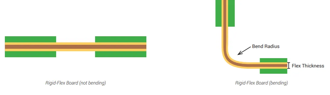
Bend areas in rigid-flex PCBs experience high tensile and compressive stresses during flexing, primarily affecting copper traces and dielectrics. The minimum bend radius determines stress levels, with tighter radii increasing strain on inner layers. Copper ductility limits repeated bending, as grain boundaries weaken under cyclic loading. Flexible dielectrics like polyimide resist cracking better than rigid ones, but coverlay thickness influences overall flexibility. Trace orientation perpendicular to the bend axis amplifies fatigue, while curved or teardrop-shaped routing distributes stress more evenly. These mechanisms explain why bend areas demand specialized design rules.
Layer count further complicates bend mechanics. Single or double-layer flex sections tolerate smaller radii than multilayers due to reduced thickness. Adhesive layers between copper and substrate can introduce shear stresses if not optimized. Thermal expansion differences during soldering or operation add to fatigue. Engineers must model these interactions using finite element analysis to predict failure modes accurately.
Solutions for Rigid-Flex PCB Bend Area Design
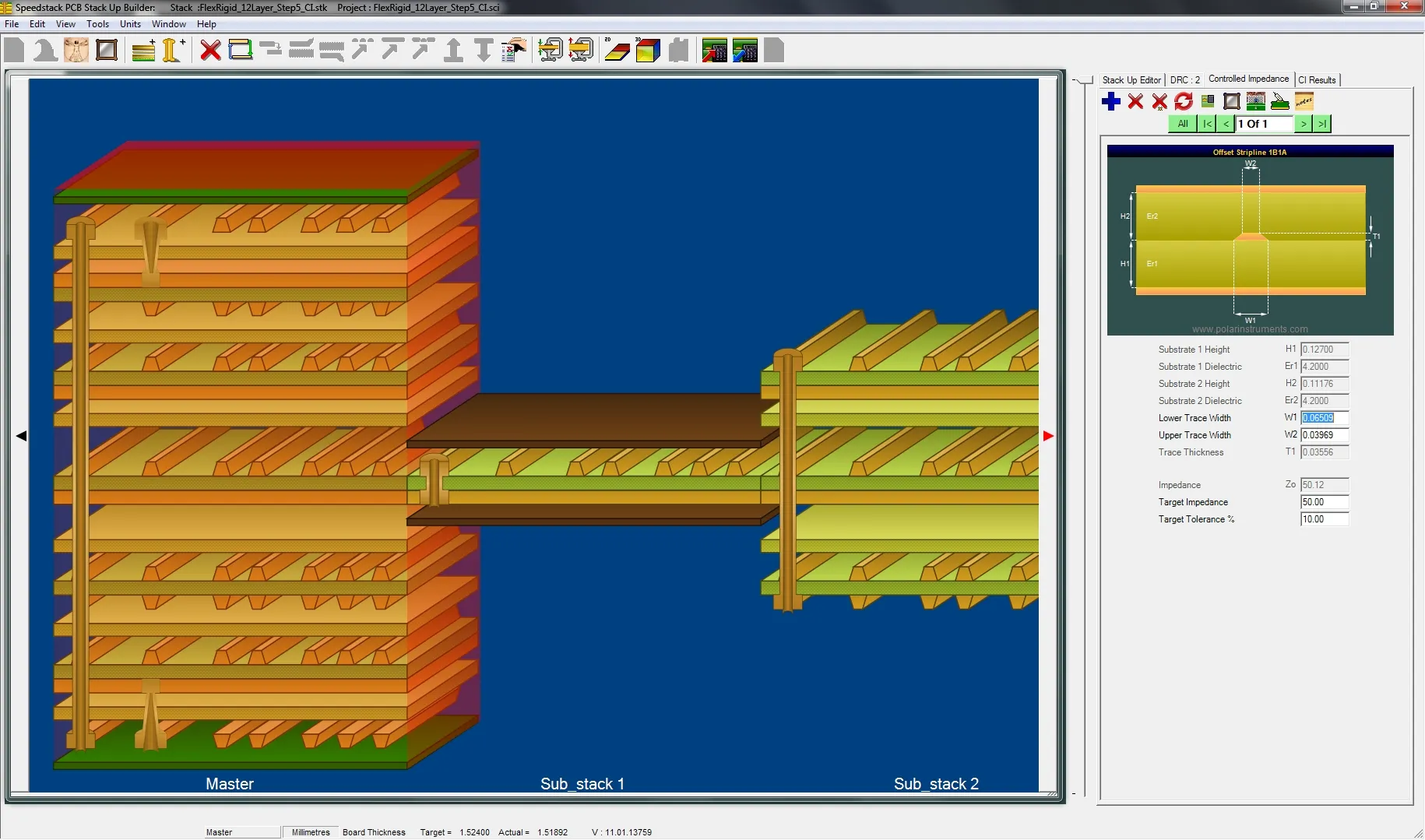
To solve rigid-flex PCB bend area design challenges, start by defining static or dynamic flexing requirements. Static bends, occurring once during assembly, allow tighter radii, while dynamic applications need larger ones to prevent fatigue. Follow IPC-2223 guidelines for bend radius based on copper foil type, layer count, and total flex thickness. For rolled annealed copper in one or two-layer designs, aim for at least six to ten times the flex section thickness. Increase this multiplier for electrodeposited copper or higher layers to accommodate reduced ductility. These challenges are closely related to overall layout strategies; learn more in our article on Overcoming Common Flex and Flex-Rigid Design Challenges in PCB Design.
Optimize trace routing in bend areas by aligning conductors parallel to the bend axis where possible. Use wider traces and curved patterns to minimize strain concentration. Avoid vias or pads in high-flex zones, as they create stress risers. Apply coverlay precisely to protect traces without adding bulk that stiffens the area. Test prototypes with bend cycle simulations to validate design margins. These rigid-flex PCB design tips enhance reliability and reduce troubleshooting needs.
Incorporate strain-relief features like hatched ground planes or filler patterns to equalize stress. Gradual width transitions from rigid to flex prevent abrupt changes. Simulate thermal profiles to ensure adhesives maintain bond strength post-reflow. Document bend specifications clearly in fabrication drawings for consistent manufacturing.
Transition Zone Design Challenges and Mechanisms
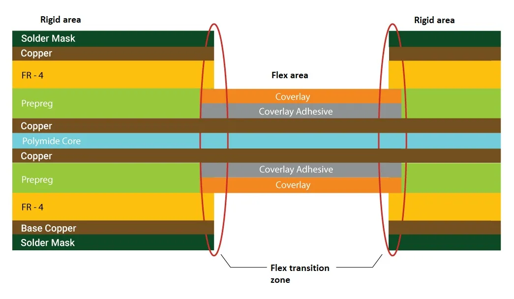
Rigid-flex PCB transition design challenges stem from the interface where rigid and flexible sections meet, creating stress concentrations due to differing moduli of elasticity. Abrupt geometry changes cause peel-up forces during bending, leading to delamination. Misaligned layers or uneven coverlay termination exacerbates cracking at edges. Vias spanning the transition experience shear from flexing, risking barrel cracks. Adhesive flow during lamination can create voids if stackup pressures vary. These factors demand precise control over outline shapes and layer alignment.
Differential CTE between rigid FR4 and flex polyimide induces warpage under temperature swings. Transition zones act as hinges, amplifying mechanical loads. Poor coverlay overlap into rigid areas leaves traces exposed to handling damage. Engineers observe these issues in cross-sections post-failure analysis, highlighting the need for structured approaches.
Best Practices for Rigid-Flex PCB Transition Design
Design transitions with smooth, tapered outlines using fillets at corners to distribute stress. Extend flex coverlay at least 0.5 mm into rigid sections for seamless protection, per IPC-2223 recommendations. Align rigid and flex outlines precisely in Gerber files, specifying separate layers for each region. Place vias outside transition zones or use blind vias to avoid spanning flex-rigid boundaries. Symmetrical stackups minimize warpage by balancing material thicknesses.
Use no-flow prepregs or low-adhesive bonding sheets in rigid sections overlying flex to prevent resin squeeze-out. Define transition zones in stackup drawings with clear cutlines. Prototype with cross-sectioning to verify interlayer adhesion. These rigid-flex PCB transition design practices reduce common failure modes like lift-off.
For multilayer boards, stagger rigidizer edges to avoid stacking faults. Incorporate anchor tabs or interlocking features for mechanical stability. Validate with thermal shock testing aligned to IPC-6013 performance classes.
Material Selection Challenges in Rigid-Flex PCBs
Rigid-flex PCB material selection involves balancing flexibility, thermal stability, and adhesion across sections. Flexible substrates must endure bending without cracking, while rigid cores provide mechanical support. Polyimide films excel in high-temperature flex areas due to low CTE and high tensile strength. FR4 laminates suit rigid sections for cost-effective rigidity and compatibility with standard processes. Adhesives bridge these materials, but choices affect bond integrity under humidity or reflow.
Challenges include adhesive outgassing during soldering, causing voids, or stiffness mismatches leading to peel. Copper foil type influences bend performance: rolled annealed offers better ductility than electrodeposited. Coverlay materials must match substrate CTE to prevent delamination. Engineers face trade-offs in cost, availability, and qualification testing. For a broader overview of flexible substrates, see our guide on Designing Flex and Rigid-Flex PCBs: A Comprehensive Manufacturing Guide.
The table below compares key options:
| Material Type | Advantages | Disadvantages | Best Applications |
|---|---|---|---|
| Adhesiveless Polyimide | Thinner profile, superior flexibility, better dimensional stability, higher reliability in thermal cycling | Higher cost, lower copper peel strength in some formulations | High-layer dynamic flex, aerospace, medical implants |
| Adhesive-Based (Acrylic/Epoxy) | Lower cost, higher initial peel strength, easier processing | Added thickness reduces bend performance, risk of outgassing/delamination at high temperatures | Cost-sensitive static applications, consumer wearables |
| No-Flow Prepregs (Rigid Areas) | Prevents resin flow into flex zones, maintains flexibility | Slightly higher material cost | Multilayer rigid-flex with tight transitions |
| Rolled Annealed (RA) Copper | Excellent ductility for dynamic flexing | More expensive than electrodeposited (ED) copper | Dynamic bend areas requiring high cycle life |
Optimizing Rigid-Flex PCB Material Selection
Select polyimide-based dielectrics for flex sections in applications exceeding 150 degrees Celsius, ensuring compliance with thermal class requirements. Pair with acrylic or modified epoxy adhesives for static flex, reserving polyimide adhesives for dynamic or high-reliability needs. FR4 cores should have high Tg for reflow stability. Verify material datasheets for peel strength exceeding 1 pound per inch minimum.
Conduct compatibility tests for CTE matching below 50 ppm per degree Celsius difference. Use adhesiveless laminates where possible to eliminate weak interfaces. Specify copper weights thinner in flex areas, like 1 oz, for easier bending. These rigid-flex PCB material selection strategies align with IPC standards and enhance durability.
Consider environmental factors: hydrolysis-resistant polyimides for humid conditions. Balance total stackup thickness to control overall flexibility.
Integrated Best Practices and Troubleshooting
Combine bend, transition, and material strategies for holistic rigid-flex PCB design. Develop stackups early, iterating with 3D models for bend simulation. Use design rule checks for minimum radii and clearances. Troubleshoot failures by sectioning samples and inspecting under microscopy for cracks or voids. Common issues like trace fractures trace back to insufficient radius; delamination to poor adhesion.
Table 1: Quick Rigid-Flex PCB Troubleshooting Guide
- Bend cracking — Tight radius — Increase to 10x thickness
- Transition delamination — Abrupt outline — Add fillets, extend coverlay
- Warpage — CTE mismatch — Symmetrical stackup
- Via failure — Flex spanning — Relocate or blind vias
Prototype iteratively, incorporating feedback from fabricators. These rigid-flex PCB design tips streamline workflows.
DFM Guidelines, Verification, and Fabrication Considerations
Strong rigid-flex dfm collaboration with your manufacturer is non-negotiable. Provide a comprehensive fabrication drawing that clearly calls out minimum bend radius, flex direction, material stackup, coverlay termination, and transition boundaries. Specify IPC-2223 and IPC-6013 class requirements upfront.
Include test coupons for flex endurance, peel strength, and thermal shock testing on every panel. Verify designs with AOI, cross-section analysis, and accelerated life testing (e.g., 1,000+ bend cycles for dynamic applications). Fabricators can recommend optimizations such as adhesiveless cores for tight bends or specific no-flow prepregs. Early DFM reviews typically reduce revision cycles by 50 % and improve first-pass yields significantly. Request impedance and continuity testing tailored to the rigid and flex zones.
Case Studies and Real-World Solutions
Case 1 – Portable Medical Diagnostic Device (Dynamic Flex)
A wearable ultrasound probe experienced copper cracking after ~5,000 cycles. Root cause: insufficient bend radius (4× thickness) on a 2-layer adhesively bonded flex. Solution: switched to adhesiveless polyimide, increased radius to 15× thickness per IPC-2223, implemented hatched ground planes, and added strain-relief slots. Cycle life exceeded 150,000 with zero field failures.
Case 2 – Aerospace Avionics Module (Static Bend + Thermal Extremes)
Warpage and transition delamination occurred during thermal vacuum testing due to asymmetric stackup and CTE mismatch. Redesign used a fully symmetric rigid-flex stackup design, no-flow prepreg in rigid sections, filleted transitions with extended coverlay, and RA copper. The board passed IPC-6013 Class 3 qualification with <0.3 % warpage and is now flying on multiple satellite programs.
Case 3 – Foldable Consumer Wearable (High-Density HDI)
Signal integrity degradation and assembly yield loss stemmed from vias in transition zones and abrupt geometry. Implementation of keep-out zones, blind vias, optimized routing, and early fabricator DFM review raised first-pass yield from 76 % to 98 % while maintaining 100 Ω differential impedance across the flex-rigid boundary.
These rigid-flex case studies demonstrate the measurable ROI of applying the techniques outlined above.
Conclusion
Mastering rigid-flex PCB design challenges in bend areas, transitions, and material selection unlocks reliable, compact electronics. Logical stackup planning, adherence to bend radii per IPC-2223, smooth transitions, and matched materials form the foundation. Electric engineers benefit from structured approaches that prevent common pitfalls like fatigue or delamination. Implementing these rigid-flex PCB troubleshooting techniques reduces risks and accelerates development. Prioritize simulation and testing for optimal results.
FAQs
Q1: What are the main rigid-flex PCB design challenges in bend areas?
A1: Bend areas face high stress from flexing, leading to copper fatigue or dielectric cracks. Key issues include inadequate minimum bend radius and perpendicular trace routing. Solutions involve using IPC-2223 guidelines for radii at least six to ten times flex thickness, curved traces, and avoiding vias. This ensures longevity in static or dynamic applications.
Q2: How do you optimize rigid-flex PCB transition design?
A2: Transitions require gradual tapers and fillets to avoid stress risers. Extend coverlay into rigid sections for protection and use symmetrical stackups to control warpage. Align layers precisely and place no spanning vias. These rigid-flex PCB design tips per industry standards prevent delamination during assembly and use.
Q3: What factors influence rigid-flex PCB material selection?
A3: Choose polyimide for flex durability and FR4 for rigid support, matching adhesives for CTE and thermal needs. Consider dynamic vs. static flexing and environmental exposure. Adhesiveless builds reduce interfaces. Proper selection aligns with IPC-6013 qualification for reliable performance.
Q4: What are essential rigid-flex PCB design tips for troubleshooting?
A4: Start with stackup reviews for balance, simulate bends, and inspect prototypes via cross-sectioning. Address warpage with CTE-matched materials and fatigue with wider traces. Document rules clearly. These practices resolve most rigid-flex PCB design challenges efficiently.
References
IPC-2223E — Sectional Design Standard for Flexible/Rigid-Flexible Printed Boards. IPC, 2020
IPC-6013D — Qualification and Performance Specification for Flexible/Rigid-Flexible Printed Boards. IPC, 2017


