Introduction
In high-speed PCB designs, differential pairs form the backbone of reliable data transmission for interfaces like USB, PCIe, and Ethernet. These pairs consist of two closely spaced traces carrying complementary signals, which reject common-mode noise and preserve signal integrity. However, transitioning layers with vias introduces challenges that can disrupt this balance. Poor via placement leads to impedance mismatches, intra-pair skew, and increased crosstalk, compromising performance at multi-gigabit speeds. Differential pair via design requires precise strategies to ensure continuity in characteristic impedance and minimal signal degradation. This article explores the principles and best practices for optimal via placement, tailored for engineers tackling signal integrity in complex multilayer boards.
Understanding Differential Pairs and Via Challenges
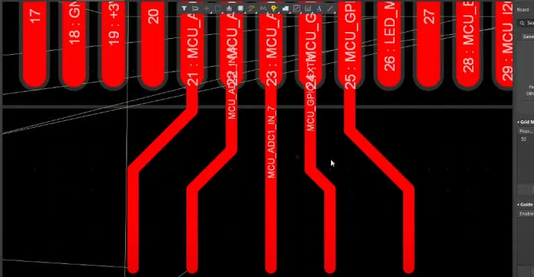
Differential pairs transmit signals as the difference between two traces, typically targeting 100-ohm differential impedance. Vias enable layer changes to optimize routing density and avoid congestion, but they create inductive and capacitive discontinuities. The via barrel acts as a stub that reflects signals if not properly managed, altering the return path and causing impedance bumps. Asymmetrical via placement exacerbates via skew differential pairs, where length differences between positive and negative traces convert differential signals to common-mode noise. Crosstalk arises when unbalanced vias couple energy unevenly between pairs or to adjacent nets. Engineers must prioritize symmetrical via placement to align electrical lengths and maintain field symmetry. Effective implementation begins with proven differential pair routing best practices to minimize via-induced discontinuities.
Why Via Placement Matters for Differential Pair Impedance and Signal Integrity
Controlled impedance ensures maximum power transfer and minimal reflections, critical for eye diagram quality and bit error rates. In differential impedance via placement, even small deviations from 100 ohms can degrade margins at frequencies above 1 GHz. Vias disrupt the uniform transmission line model, with stub lengths beyond a fraction of the wavelength causing significant insertion loss. Minimizing crosstalk differential pairs involves shielding fields through symmetric geometry, preventing far-end or near-end coupling. Industry standards like IPC-2221C outline routing guidelines that emphasize these controls for high-speed performance. Neglecting via optimization results in redesign iterations, higher EMI emissions, and failed compliance tests.
Technical Principles Governing Via Effects
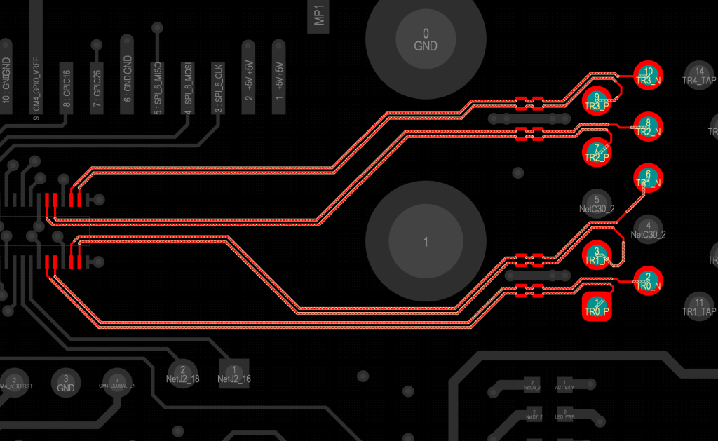
Vias introduce parasitic inductance from the barrel and capacitance from the antipad clearance in the plane. For differential pairs, the odd-mode impedance depends on the coupled fields between traces, which vias can unbalance if not mirrored precisely. Symmetrical via placement keeps the loop area consistent, preserving the differential mode propagation. Via skew differential pairs occurs when one via transitions farther or uses a different drill size, shifting phase and inducing skew beyond 10 ps per inch tolerances. Crosstalk mechanisms include capacitive coupling through overlapping fields and inductive coupling via shared return paths. Simulations using time-domain reflectometry reveal these effects, showing return loss peaks at via locations without mitigation.
Suggested Reading:
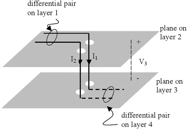
The return current flows through nearby planes, so via placement must avoid splitting planes or creating long detours. Antipad sizing affects capacitive loading; oversized antipads increase fringing fields, while undersized ones risk shorts. Stub resonance frequency drops with length, turning vias into filters at operating harmonics. Backdrilling removes unused stubs, aligning impedance closer to traces. These principles guide differential pair via design toward predictable behavior across the stackup.
Best Practices for Symmetrical Via Placement and Differential Line Placement
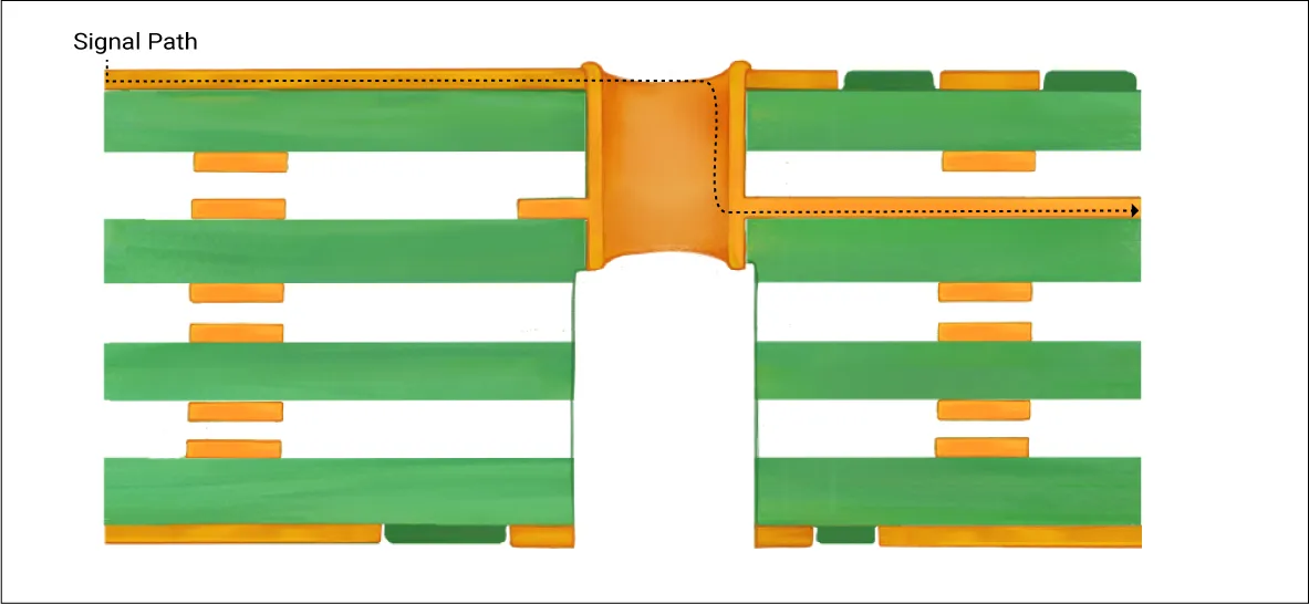
Start with stackup planning to minimize layer transitions, routing pairs on outer layers where possible. When vias are necessary, position them equidistant from trace edges, maintaining the pair's edge-coupled geometry. Use identical via diameters, drill depths, and plating for both lines to ensure symmetry. Symmetrical via placement not only equalizes lengths but also balances parasitics, reducing mode conversion. Space vias from other nets by at least three times the pair spacing to minimize crosstalk differential pairs. Grid-align multiple vias for serpentine length matching, avoiding diagonal offsets.
Incorporate filled or blind vias for inner layer transitions to shorten stubs. Backdrilling targets stub lengths below one-tenth wavelength, often under 20 mils for 10 Gbps signals. Verify with field solvers pre-layout, targeting less than 5% impedance variation. IPC-6012F specifies performance criteria for vias in rigid boards, including plating uniformity that supports these practices. Route pairs broadside-coupled on inner layers if microstrip is unavailable, adjusting dielectric thickness for impedance.
Length-tune traces post-via with smooth meanders, keeping amplitude below 20% of spacing. Ground via stitching around pairs at lambda-quarter intervals to stabilize return paths. These steps in differential impedance via placement yield robust designs resilient to fabrication tolerances.
The table below summarizes recommended dimensions by data rate (assuming typical 8–10 mil drill vias on FR-4 or low-loss laminates):
| Data Rate | Max Intra-Pair Via Spacing | Recommended Ground Via Distance from Signal Via | Max Allowable Stub Length | Notes |
|---|---|---|---|---|
| ≤10 Gbps | ≤15 mils | 1.5–2× via diameter | <30 mils | Basic symmetry usually sufficient |
| 16–28 Gbps | ≤10 mils | 1.5× via diameter | <11 mils | Backdrilling strongly recommended |
| 32–112 Gbps | ≤8 mils | ≤1.5× via diameter | <10 mils (often <7 mils) | Per-layer backdrilling or blind/microvias required |
Space signal vias at least 3× the pair spacing from unrelated nets to limit crosstalk. Use smooth length-tuning meanders (amplitude <20% of spacing) after the via transition. Target less than 5% impedance variation through the transition, verified by 3D field solvers. These practices in differential impedance via placement produce robust designs that tolerate normal fabrication variation.
Advanced Techniques and Troubleshooting
For dense boards, microvias offer shorter stubs but demand tighter tolerances per IPC guidelines. Filled vias enhance reliability under thermal stress by reducing voids. When skew persists, measure intra-pair delay with vector network analyzers and adjust high-speed routing. Common pitfalls include via-in-pad without plugged protection, leading to solder wicking, or asymmetric antipads causing field tilt. Crosstalk spikes signal when pairs cross layers orthogonally without ground shielding. Troubleshooting involves isolating via contributions via de-embedding in simulations.
Case in point: a 12-layer board with PCIe Gen4 pairs showed 15% eye closure from 5-mil via offset; symmetrizing and backdrilling restored height margins. Always prototype critical nets for validation.
Simulation and Modeling of Differential Via Transitions
Simulation is non-negotiable for high-speed designs. Use 3D full-wave solvers (HFSS, CST Microwave Studio) or SI-specific tools (HyperLynx, Cadence Sigrity, ADS) to model the exact via geometry, including pads, antipads, ground stitching, and stack-up materials. Extract S-parameters or perform TDR analysis to quantify impedance profiles, insertion loss, return loss, and mode conversion (SCD21).
Target < –15 dB return loss and minimal mode conversion through the via transition up to the Nyquist frequency (e.g., 16 GHz for 32 GT/s). Simulate multiple fabrication corners (etch tolerances, dielectric variation) to ensure robustness. Time-domain eye diagrams from channel simulation reveal the combined impact on BER and eye height. Early simulation of differential pair via placement prevents costly layout iterations and correlates closely with VNA measurements on prototypes.
Case Study: Building a 28 Gbps+ Differential Channel
A 12-layer board for a PCIe Gen4/Gen5 accelerator card required 28 Gbps differential channels with multiple layer transitions. Initial layout exhibited a 5-mil via offset between P and N legs, producing approximately 15% eye closure, elevated mode conversion, and a return-loss peak near 14 GHz.
The team redesigned with perfectly symmetrical via placement (identical drill, pad, and antipad), added four ground stitching vias at 1.5× via diameter, implemented per-layer backdrilling to limit stubs to <10 mils, and verified the transition in CST. Post-layout simulation showed impedance variation reduced to <3%, eye height improved by 38%, and BER margins comfortably below 10⁻¹². Prototype boards measured with a VNA and real-time oscilloscope correlated within 5% of simulation. The final design passed compliance testing on the first fabrication run, demonstrating the ROI of rigorous via placement for differential pairs and stitching practices.
Conclusion
Mastering via placement for differential pairs hinges on symmetry, minimal discontinuities, and rigorous verification. By adhering to principles of balanced parasitics and controlled stubs, engineers achieve stable impedance and low skew. These practices mitigate crosstalk, ensuring signal integrity across high-speed channels. Integrating standards like IPC-2221C elevates designs from functional to optimal. Prioritize simulation and DFM checks early to streamline fabrication.
FAQs
Q1: What is symmetrical via placement in differential pair via design?
A1: Symmetrical via placement positions vias for both traces of a differential pair at identical locations relative to the pair centerline, using matching sizes and depths. This maintains equal electrical lengths and balanced fields, preventing skew and mode conversion. It preserves 100-ohm differential impedance through layer changes. Engineers achieve this by mirroring geometries in layout tools, verifying with 3D solvers for parasitics under 1 ohm deviation.
Q2: How does via skew affect differential pairs?
A2: Via skew differential pairs introduces phase differences between signals, converting differential mode to common-mode noise that receivers reject poorly. Even 2 ps skew at 10 Gbps closes eye diagrams by 10-20%. Asymmetric via locations or stub lengths cause this, amplified by frequency. Mitigate by equalizing via counts and positions, length-tuning traces, and using backdrilling for uniform transitions.
Q3: Why is minimizing crosstalk critical in differential pair routing?
A3: Minimizing crosstalk differential pairs prevents far-end distortion from coupled aggressors, preserving bit error rates below 10^-12. Vias exacerbate coupling if antipads overlap fields or stubs resonate. Maintain 3x spacing rules, orthogonal layer routing, and ground stitching. Symmetrical designs confine fields tightly, reducing NEXT and FEXT by over 20 dB.
Q4: What role does backdrilling play in differential impedance via placement?
A4: Backdrilling removes via stubs beyond the signal layers, eliminating resonances that bump impedance by 20-50 ohms. It aligns via transition impedance to trace values, vital for frequencies over 5 GHz. Specify depths precisely to avoid over-drill, per performance specs. This technique enhances return loss by 10 dB, ideal for long-reach channels.
References
IPC-2221C — Generic Standard on Printed Board Design. IPC, 2023
IPC-6012F — Qualification and Performance Specification for Rigid Printed Boards. IPC, 2023