Introduction
Industrial sensor PCB assembly plays a critical role in manufacturing devices that monitor environmental conditions, machinery performance, and process variables in factories, oil fields, and transportation systems. These printed circuit boards integrate sensitive components like pressure transducers, temperature probes, and accelerometers, demanding high precision to ensure accurate data capture amid vibrations, humidity, and temperature extremes. Proper assembly techniques prevent failures that could lead to downtime or safety risks in automated systems. Surface mount technology dominates due to miniaturization needs, while through-hole methods add mechanical strength for rugged applications. Reflow soldering and wave soldering form the backbone of these processes, with automated optical inspection verifying quality. This guide explores the essentials of industrial sensor PCB assembly, offering practical insights for electric engineers optimizing reliability and performance.
What Is Industrial Sensor PCB Assembly and Why It Matters
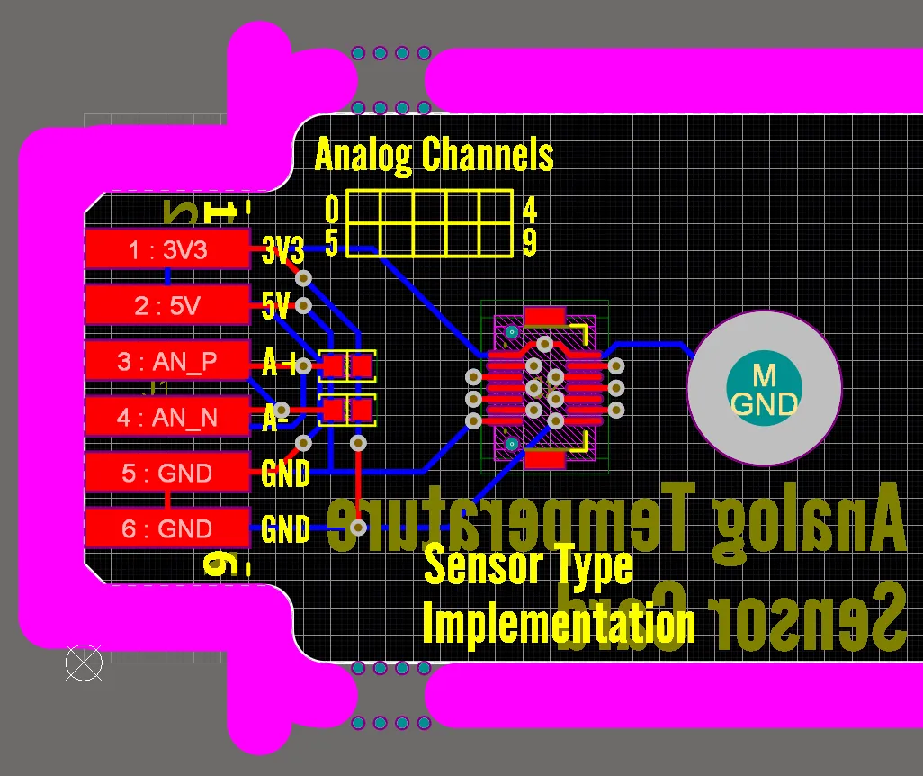
Industrial sensor PCB assembly refers to the process of populating bare boards with electronic components to create functional sensor modules. It encompasses solder paste application, component placement, soldering, and inspection tailored to sensors' unique requirements, such as low noise for signal integrity and robustness against mechanical stress. SMT assembly handles fine-pitch ICs and passives, enabling compact designs, whereas through-hole assembly secures larger connectors and leads for vibration-prone setups. Engineers must balance density with durability, as sensors often operate in class 3 environments per industry benchmarks.
This assembly matters because industrial sensors drive Industry 4.0, feeding data to control systems for predictive maintenance and efficiency. Faulty joints from poor reflow soldering can amplify noise or drift signals, causing erroneous readings in critical applications like leak detection or structural health monitoring. Wave soldering ensures strong bonds in mixed-technology boards, but misalignment risks signal crosstalk. Automated optical inspection catches defects early, reducing field failures that cost thousands in recalls. Ultimately, compliant assembly extends sensor lifespan, aligning with demands for zero-defect production in high-stakes sectors.
Key Technical Principles in Industrial Sensor PCB Assembly
The foundation of industrial sensor PCB assembly lies in surface mount technology, where solder paste is screen-printed onto pads via stencils with precise apertures matching component footprints. Pick-and-place machines then position tiny resistors, capacitors, and sensor dies with micron accuracy, critical for maintaining impedance control in analog circuits. Reflow soldering follows in a conveyor oven, where the board passes through preheat, soak, reflow, and cool zones to form reliable metallurgical bonds without damaging heat-sensitive sensors. Profile optimization prevents overheating, which could degrade piezoelectric elements or shift calibration. For high-reliability requirements in harsh conditions, also consult our article on Designing High Reliability Industrial Sensor PCBs for Harsh Environments which covers material and protection strategies that affect assembly processes.
Through-hole assembly complements SMT by inserting component leads into drilled vias, often for power transistors or hermetic packages in harsh environments. Wave soldering dips the board's underside into a molten solder fountain, creating fillet joints that withstand shear forces from vibrations. Dual-wave systems handle mixed assemblies, with a turbulent first wave cleaning holes and a laminar second forming smooth fillets. Preheating minimizes thermal shock, ensuring vias fill completely without voids that compromise thermal dissipation in power-hungry sensors.
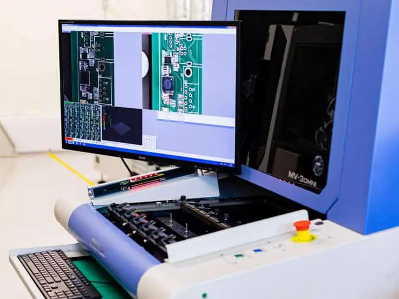
Automated optical inspection scans boards post-soldering using high-resolution cameras and algorithms to detect anomalies like bridging, misalignment, or insufficient solder volume. Multi-angle lighting reveals shadows on tall components, while 3D profiling measures joint heights against tolerances. For industrial sensors, AOI verifies BGA balls under vision chips, preventing intermittent opens from handling stress. Integration with X-ray for hidden defects enhances yield, as visual alone misses subsurface issues.
Adherence to J-STD-001J ensures soldering processes meet criteria for materials, methods, and verification, particularly for reflow and wave profiles in sensor assemblies.
SMT, Through-Hole, and Mixed Assembly Comparison for Sensors
| Assembly Type | Best For | Advantages | Challenges | Typical Sensor Applications |
|---|---|---|---|---|
| SMT Assembly | Fine-pitch ICs, passives, compact designs | High density, fast production, low parasitics | Sensitive to thermal shock, harder rework | MEMS accelerometers, signal conditioners |
| Through-Hole | Connectors, power components, rugged builds | Excellent mechanical strength, vibration resistance | Lower density, slower process | Heavy-duty pressure sensors, terminal blocks |
| Mixed Assembly | Most industrial sensors | Combines density + strength | Sequencing complexity, thermal management | Hybrid sensor modules with both fine-pitch and robust connectors |
Mixed-technology boards are most common, requiring careful process sequencing to protect SMT components during wave soldering.
Practical Best Practices for Industrial Sensor PCB Assembly
Start with design for manufacturability by spacing components adequately for stencil alignment and inspectability, especially around tall sensors that shadow neighbors. Select FR-4 or polyimide substrates with controlled impedance traces to preserve signal fidelity, and incorporate fiducials for machine registration. Solder paste choice favors no-clean types with fine particle size for 01005 passives, applied at 75-85% paste-to-pad volume to avoid starving or excess during reflow.
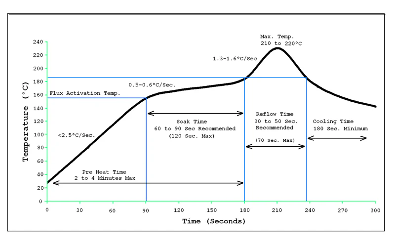
For SMT assembly, validate stencil thickness, typically 100-125 microns for fine pitch, and use vacuum tweezers for manual tweaks on prototypes. Reflow profiles ramp at 1-3°C/s to 150°C preheat, hold for flux activation, peak at 235-260°C for lead-free alloys, and cool below 170°C rapidly to minimize intermetallic growth. Nitrogen atmospheres reduce oxidation on sensor leads, improving wetting on copper pads exposed to humidity.
In through-hole PCB assembly, wave soldering demands fluxers with even spray for hole penetration, followed by defluxing to prevent ionic residues that corrode sensor contacts. Post-wave cleaning uses deionized water sprays, verified by resistivity meters above 1 MOhm-cm. Mixed boards benefit from selective soldering for sensitive areas, avoiding broad wave exposure.
Automated optical inspection should occur inline after reflow and wave, programmed for class 3 criteria per IPC-A-610J, flagging tombstoning from uneven paste or solder balls from splatter. Follow with functional testing, including in-circuit probes for sensor outputs and boundary scans for BGA integrity. Conformal coating with acrylic or silicone protects against moisture ingress, applied post-inspection via selective spray to avoid trapping defects.
Inspection and Quality Control (AOI, X-Ray, ICT)
Inline automated optical inspection (AOI) after reflow and wave uses 3D imaging and multi-angle lighting to detect bridging, misalignment, insufficient solder, or tombstoning per IPC-A-610 Class 3 criteria. X-ray inspection is essential for hidden defects in BGAs and through-hole fills, targeting void rates below 25%.
In-circuit testing (ICT) and functional testing verify sensor outputs, boundary scan for BGAs, and overall module performance. Combining AOI, X-ray, and ICT catches defects early, dramatically improving yield in high-volume sensor production.
Troubleshooting Common Issues in Industrial Sensor PCB Assembly
Warpage from reflow thermal mismatch between copper layers and substrate causes stencil lift-off, leading to open joints on corner components. Mitigate by symmetric stackups, low-CTE materials, and bow/warp specs under 0.75% per board size. Measure with shadow moiré interferometry pre-assembly to predict issues.
Solder voids in BGA sensors arise from outgassing flux or poor paste release, detectable via X-ray as dark spots exceeding 25% area. Optimize ramp rates and vacuum reflow for critical devices, or switch pastes with lower viscosity. Tombstoning lifts passives due to uneven wetting; balance paste volume and preheat to synchronize melting.
Wave soldering bridges through-hole pins from flux drag-out or high solder pot temps; adjust conveyor angle to 6-8° and use low-solids flux. Post-solder tilt boards to drain excess, then AOI for cleanup. Vibration testing post-assembly simulates industrial loads, revealing cracked fillets early.
For signal noise in sensors, inspect ground planes for voids disrupting shielding, rework per IPC-7711 guidelines with hot air stations. Always bake hygroscopic components pre-assembly to J-STD-020 levels, preventing popcorning.
Suggested Reading: Optimizing Industrial Sensor PCB Layout for Signal Integrity and Noise Reduction
Real-World Case Studies and Yield Improvement Tips
In a predictive maintenance sensor line, switching to optimized reflow profiling and vacuum-assisted BGA soldering reduced void rates from 35% to under 10%, boosting first-pass yield by 18% and cutting field returns.
A vibration monitoring module achieved higher reliability by combining selective soldering, silicone conformal coating, and rigorous AOI/X-ray, surviving extended shake-table testing with zero failures. Yield improvement tips include statistical process control on paste volume and thermal profiles, supplier audits for consistent materials, and continuous feedback loops between design and assembly teams.
Conclusion
Industrial sensor PCB assembly demands precision across SMT assembly, through-hole assembly, reflow soldering, wave soldering, and automated optical inspection to deliver robust, reliable modules. Engineers achieve this through standards-compliant processes, design foresight, and vigilant troubleshooting. Key practices like profile control, inline AOI, and conformal protection minimize defects in demanding environments. By prioritizing these elements, teams ensure sensors perform accurately, supporting seamless industrial operations.
FAQs
Q1: What distinguishes SMT assembly from through-hole assembly in industrial sensor PCBs?
A1: SMT assembly places components directly on surface pads for density and speed, ideal for fine-pitch sensors, using reflow soldering to melt paste uniformly. Through-hole assembly inserts leads into holes for mechanical strength, suited to connectors enduring vibration, and relies on wave soldering for fillet formation. Mixed boards combine both, requiring careful sequencing to avoid damaging SMT parts during wave exposure. Automated optical inspection verifies both joint types post-process.
Q2: How does reflow soldering impact industrial sensor PCB assembly reliability?
A2: Reflow soldering melts solder paste in controlled zones to form intermetallics without stressing sensors, but improper profiles cause voids or delamination. Preheat activates flux evenly, reflow peaks ensure wetting, and rapid cool prevents brittle phases. Nitrogen use cuts dross, enhancing joint life in humid settings. Per J-STD-001J, verification includes thermal profiling and shear testing for class 3 assemblies.
Q3: Why is automated optical inspection essential in industrial sensor PCB assembly?
A3: AOI detects bridges, misalignments, and insufficient solder on dense sensor boards faster than manual checks, using 3D algorithms for volume accuracy. It flags issues like BGA head-in-pillow before functional test, boosting yield. Programming for IPC-A-610J class 3 criteria catches vibration-prone defects early. Inline placement reduces escapes, critical for high-volume sensor production.
Q4: What are common wave soldering challenges in through-hole industrial sensor PCBs?
A4: Wave soldering struggles with solder skips in deep vias or bridging on dense pins, often from flux starvation or drag. Preheat boards uniformly to expand holes, and use dual waves for cleaning then filleting. Clean residues promptly to avoid corrosion on sensor traces. AOI post-wave ensures fillet heights meet specs, preventing intermittent failures.
References
IPC-A-610J - Acceptability of Electronic Assemblies. IPC, 2024
IPC J-STD-001J - Requirements for Soldered Electrical and Electronic Assemblies. IPC, 2024


