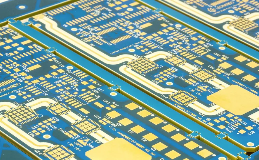
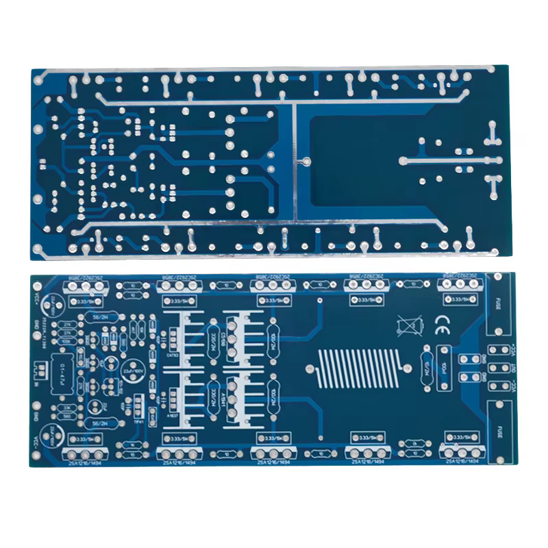
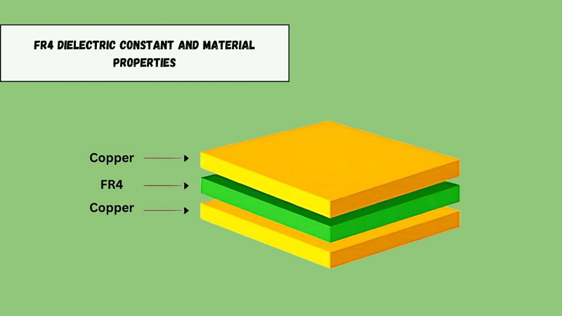
Mastering PCB Silkscreen Design for Clear and Efficient Boards
Learn how to design effective PCB silkscreen layers for better assembly, testing, and maintenance. This guide covers legibility, industry standards, and practical optimization tips.
Learn safe DIY PCB recycling methods to extract copper and recover gold from e-waste. This guide details mechanical and chemical processes for recycling circuit boards at home.
A comprehensive guide for engineers on choosing PCB drill bits, covering material types (carbide vs. HSS), sizes, and applications for FR-4 and microvias to ensure precise fabrication.
Master controlled depth drilling for better DIY PCB signal integrity. This guide offers practical tips and back drilling basics to enhance your home PCB projects.
Learn essential techniques for 50 ohm impedance control in PCB stackup design, covering microstrip and stripline calculations, material selection, and best practices for high-frequency applications.
Discover the critical relationship between PCB trace width and impedance in high-speed designs. Learn how to calculate trace width for desired impedance and optimize signal integrity.
Learn how to determine the minimum PCB trace width for 20A currents using IPC-2221 standards, considering copper thickness, temperature rise, and layer placement.
Explore the critical role of PCB dielectric thickness in signal integrity, impedance control, and high-speed design, including FR-4 standards and calculation methods.
Learn how strategic placement, current capacity, and inductance management of power plane vias are crucial for robust PCB signal integrity.
Delve into how via aspect ratio influences PCB reliability, covering calculation methods, common issues with high aspect ratios, and best practices for optimal design and manufacturing.
Learn essential op-amp PCB layout guidelines, EMI reduction techniques, ground plane design, and decoupling capacitor placement for clean, high-performance analog circuits.
Learn the essentials of HDI PCB design for 5G applications with a focus on high frequency challenges and solutions. Gain practical tips on material selection, stackup planning, and signal integrity for optimal 5G performance.