Introduction
Solar inverters play a vital role in photovoltaic systems by converting direct current from solar panels into alternating current for grid or home use. The printed circuit boards (PCBs) within these inverters handle high voltages, currents, and thermal loads, making them susceptible to various faults. Effective solar inverter PCB troubleshooting ensures system reliability, reduces downtime, and extends equipment life. Engineers often encounter issues like overheating and component failures that demand systematic diagnosis. This article provides a practical approach to diagnosing PCB faults, focusing on common problems and hands-on methods. By following structured steps, electric engineers can identify and address inverter PCB repair needs efficiently.
Why Solar Inverter PCBs Matter and Common Issues
Solar inverter PCBs integrate power electronics, control circuits, and protection components under demanding conditions such as temperature cycling and high humidity. Failures in these boards can lead to complete system shutdowns, safety hazards, or reduced energy output. Common PCB issues include solder joint cracks from thermal stress, capacitor degradation, and trace delamination. Power semiconductors like MOSFETs or IGBTs often fail due to overcurrent or voltage spikes. Environmental factors exacerbate these problems, causing corrosion or conductive anodic filamentation in humid environments. Recognizing these patterns is the first step in effective diagnosing PCB faults.
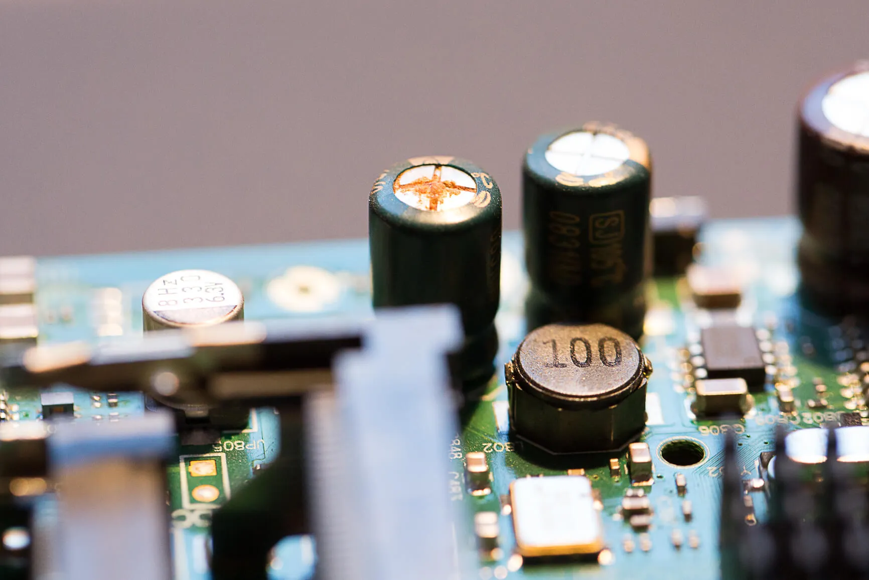
Overheating stands out as a primary concern, resulting from inadequate thermal management or high current densities in traces. Bulging or leaking electrolytic capacitors signal electrolyte evaporation under heat. Short circuits may arise from solder bridges or damaged insulation between high-voltage paths. Open circuits often stem from cracked vias or lifted pads after repeated thermal expansion. Isolation faults, common in moist conditions, indicate ground leaks or arcing paths. These issues highlight the need for proactive solar inverter PCB troubleshooting to maintain performance.
Root Causes of PCB Failures in Solar Inverters
Thermal cycling induces coefficient of thermal expansion mismatches between copper traces, substrates, and components, leading to cracks. High power density generates I squared R losses, concentrating heat in narrow traces or vias. Electrical transients from grid fluctuations or lightning can exceed component ratings, causing avalanche breakdown in semiconductors. Poor creepage and clearance distances foster arcing in high-voltage sections. Material degradation, such as reduced glass transition temperature in laminates, promotes warpage under load. Understanding these mechanisms guides precise inverter PCB repair strategies.
Electromagnetic interference from fast-switching circuits induces noise in control signals, mimicking faults. Humidity penetrates conformal coatings, accelerating corrosion on exposed pads or pins. Manufacturing defects like voids in solder joints weaken mechanical integrity over time. Overloaded power planes cause electromigration, thinning conductors gradually. These causes often interconnect, where initial overheating accelerates subsequent electrical failures. Engineers must isolate primary triggers during diagnosis.
Step-by-Step Guide to Diagnosing PCB Faults
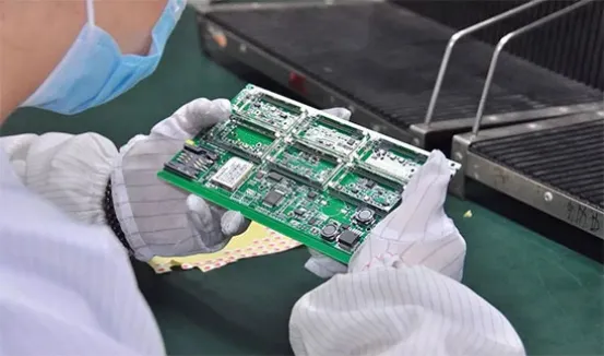
Begin troubleshooting with safety protocols: disconnect power, discharge capacitors, and use insulated tools to avoid shocks. Perform a thorough visual inspection under magnification for discoloration, cracks, or residue. Check for physical damage like burnt traces or displaced components. Verify mechanical integrity of connectors and heatsinks. Document findings with photos for reference. This initial pass reveals up to 70 percent of obvious common PCB issues without tools.
Next, employ isolation techniques to narrow down fault zones. Power off the board and segment it into power, control, and signal sections. Test continuity across each block to identify opens. Probe for shorts between power rails and ground. Measure resistance values against schematics where available. Systematic division prevents overlooking interconnected failures.
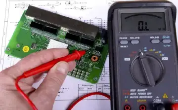
Multimeter testing for PCBs forms the core of electrical diagnosis (detailed in our PCB troubleshooting tools guide). Set the multimeter to diode mode for semiconductor junctions, expecting forward drops around 0.6 to 0.7 volts for silicon devices. Switch to continuity for traces, beeping on low resistance paths under 50 ohms. Check for shorts by measuring between adjacent nets, aiming for megaohms in isolation. Measure capacitor ESR indirectly via discharge time or in-circuit resistance. Voltage checks under partial power-up confirm bias supplies. These steps pinpoint solar inverter PCB troubleshooting targets efficiently.
Advanced Techniques for Inverter PCB Repair
Thermal imaging cameras detect hotspots indicative of high-resistance joints or failing components. Oscilloscope probing reveals signal integrity issues like ringing or distortion in gate drives. In-circuit testing fixtures validate passive values without desoldering. X-ray inspection uncovers hidden voids in BGAs or thick copper layers. Functional simulation on benches mimics operating conditions safely. Combining these elevates diagnosing PCB faults beyond basic checks.
For repair, adhere to soldering standards like J-STD-001 for joint quality, ensuring fillet shapes and wetting. Replace components with equivalents rated for voltage and temperature margins. Rework high-current traces by plating or jumper wires sized per current capacity. Apply fresh conformal coating post-repair to combat environmental ingress. Bake boards pre-assembly if moisture suspected. Verified repairs demand full system testing under load.
Prevention Best Practices
Design PCBs with heavy copper layers for current handling (see our power supply PCB trace routing best practices) and thermal vias arrays for dissipation. Segregate high-voltage areas with slots meeting clearance rules. Select high-Tg laminates stable above operating peaks. Implement robust filtering for transients and EMI. During assembly, follow IPC-A-610 criteria for joint acceptability. Routine maintenance includes thermal cycling checks and insulation resistance tests. These practices minimize recurring common PCB issues.
Conclusion
Solar inverter PCB troubleshooting demands a methodical blend of visual, electrical, and thermal diagnostics. Addressing common issues like thermal cracks and shorts promptly restores functionality and safety. Multimeter testing for PCBs proves indispensable for quick fault isolation. By applying these practical steps, engineers enhance system uptime and reliability. Prevention through standards-compliant design further reduces failures. Mastering these approaches equips teams for sustained solar energy performance.
FAQs
Q1: How do I start solar inverter PCB troubleshooting?
A1: Begin with power isolation and visual inspection for burns, cracks, or bulging parts. Use a multimeter in continuity mode to check traces and shorts between rails. Probe components for expected diode drops. Segment the board into zones for targeted testing. This sequence identifies most diagnosing PCB faults rapidly, often without advanced gear. Follow up with thermal scans if heat-related issues persist.
Q2: What are the most common PCB issues in solar inverters?
A2: Solder joint cracks from thermal cycling, capacitor failures from heat, and trace overheating top the list. Shorts from arcing or bridges disrupt power flow. Corrosion in humid setups causes isolation faults. Delamination weakens structural integrity. Early detection via routine checks prevents escalation in inverter PCB repair needs.
Q3: How effective is multimeter testing for PCBs in inverters?
A3: Highly effective for static checks like continuity, shorts, and basic component health. Diode tests verify semiconductors; resistance confirms passives. In-circuit limits accuracy for some parts, but isolates 80 percent of opens or shorts. Pair with schematics for precision in solar inverter PCB troubleshooting. Avoid powered tests without isolation to prevent damage.
Q4: Can I repair a faulty solar inverter PCB myself?
A4: Yes, for accessible faults like bad capacitors or joints, using proper soldering per standards. Diagnose first with multimeter, replace parts, and retest. Complex issues like multilayer delamination require professional rework. Ensure safety and matching components. This approach succeeds in many inverter PCB repair scenarios for experienced engineers.
References
IPC-6012E — Qualification and Performance Specification for Rigid Printed Boards. IPC, 2018
IPC-A-610H — Acceptability of Electronic Assemblies. IPC, 2019
J-STD-001H — Requirements for Soldered Electrical and Electronic Assemblies. IPC/JEDEC, 2018


