Introduction
In modern high-speed electronics, maintaining precise control over PCB impedance is essential to ensure reliable signal transmission and minimize losses. As data rates continue to increase, even minor deviations in characteristic impedance can lead to reflections, crosstalk, and degraded performance. Advanced simulation and modeling techniques have become indispensable tools for electric engineers tackling these challenges. PCB simulation software enables predictive analysis before fabrication, allowing for optimized designs that meet stringent requirements. This article explores impedance modeling, electromagnetic simulation, signal integrity analysis, and finite element analysis as key methods to achieve controlled impedance. By leveraging these approaches, engineers can enhance signal integrity analysis and reduce iteration cycles in PCB development.
Understanding PCB Impedance Control and Its Importance
Characteristic impedance in a PCB trace is determined by the interaction of inductance and capacitance along the transmission line, primarily influenced by trace geometry, dielectric materials, and stackup configuration. Controlled impedance ensures that the signal propagates with minimal distortion, which is critical for applications operating above 1 GHz. Without proper impedance control, mismatches cause signal reflections that degrade eye diagrams and increase bit error rates. Industry standards like IPC-2141 provide guidelines for designing transmission lines with predictable impedance values. For electric engineers, mastering impedance control directly impacts the success of multilayer boards in telecommunications, computing, and automotive systems. Signal integrity analysis through simulation verifies these designs early, preventing costly prototypes.
Impedance control matters because high-speed signals behave as transmission lines where wavelength approaches trace lengths, amplifying discontinuity effects. Variations in manufacturing tolerances, such as etch factor or dielectric thickness, can shift impedance by several ohms. Electromagnetic simulation tools model these effects accurately, offering insights into real-world behavior. Engineers must consider both single-ended and differential pair impedances, as differential signaling is common in USB, PCIe, and DDR interfaces. By integrating impedance modeling into the design flow, teams achieve compliance with performance specs and improve yield. Ultimately, these techniques bridge the gap between theoretical calculations and fabricated boards. For detailed guidance on layer arrangement to support these targets, see our guide on high-speed PCB stackup design.
Core Principles of Impedance in PCB Design
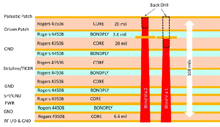
The characteristic impedance Z0 of a microstrip or stripline is governed by the formula Z0 = sqrt(L/C), where L is inductance per unit length and C is capacitance per unit length. Trace width, thickness, and separation from reference planes dictate these parameters, while dielectric constant (Dk) and loss tangent (Df) affect propagation. In multilayer PCBs, asymmetric stackups introduce coupling between layers, complicating predictions. Finite element analysis discretizes the geometry into meshes to solve Maxwell's equations numerically, providing precise field distributions. This method excels in modeling complex structures like vias and bends where 2D approximations fail. Understanding these principles forms the foundation for effective impedance modeling.
Material properties play a pivotal role, as low-Dk dielectrics reduce capacitance and increase impedance for given geometries. However, trade-offs exist with mechanical stability and cost. Electromagnetic simulation captures frequency-dependent behaviors, such as skin effect and dielectric dispersion, which simple calculators overlook. Signal reflections occur when impedance discontinuities exceed 10% of Z0, leading to voltage overshoot. Engineers use time-domain reflectometry (TDR) concepts in simulations to visualize these mismatches. Adhering to standards like IPC-2221 ensures designs account for fabrication variations systematically.
Essential Tools for PCB Impedance Simulation
Modern PCB simulation software integrates seamlessly into design flows, offering everything from quick stackup calculators to full-wave solvers. Popular professional tools include:
- Ansys SIwave: Strong in multiphysics SI/PI/EMI analysis for PCBs and packages, with automated decoupling and full-wave extraction.
- Cadence Sigrity / Allegro SI: Excellent for constraint-driven high-speed design, system-level channel simulation, and integration with layout tools.
- Siemens HyperLynx: User-friendly for signal and power integrity, with good support for pre- and post-layout analysis.
- Keysight ADS / PathWave: Popular for RF/microwave and advanced SerDes channel simulation using IBIS-AMI models.
- Simbeor: Specialized, measurement-validated EM solver focused on accurate interconnect modeling for high-speed links.
- Altium Designer: Integrated impedance calculation and basic SI features, suitable for many workflows.
These tools vary in strengths—some emphasize speed and integration, others raw EM accuracy or ease of use. A typical pros/cons comparison might highlight Ansys and Cadence for complex 3D structures versus more accessible options for quicker iterations. Choosing the right tool depends on design complexity, team expertise, and budget.
Advanced Simulation Techniques for Impedance Control
PCB simulation software employs quasi-static 2D field solvers for initial impedance calculations on uniform traces, offering rapid feedback during layout. For more accuracy, full-wave 3D electromagnetic simulation solves Maxwell's equations across the entire structure, capturing higher-order modes and radiation. Finite element analysis (FEA) divides the model into tetrahedral elements, iteratively refining solutions for irregular geometries like coupled lines or embedded components. These tools integrate seamlessly with design environments, enabling pre-layout optimization. Signal integrity analysis extends beyond impedance to include crosstalk, insertion loss, and return loss predictions. Engineers benefit from parametric sweeps to explore tolerance impacts efficiently.
Method of moments (MoM) and finite difference time domain (FDTD) complement FEA in electromagnetic simulation suites. MoM suits planar structures, while FDTD handles dispersive materials over broad bandwidths. Hybrid approaches combine these for comprehensive modeling, reducing computational overhead. In practice, mesh convergence studies validate results, ensuring accuracy within 2-5% of measurements. Impedance modeling at this level reveals subtle effects like via stub resonances in high-density interconnects (HDI). These techniques empower engineers to design for 50-ohm single-ended or 100-ohm differential pairs reliably.
Detailed Impedance Modeling Approaches
Impedance modeling begins with synthetic field solver models that approximate stackup parameters using closed-form equations derived from conformal mapping. These suffice for symmetric striplines but underestimate edge effects in microstrips. Transitioning to 3D models incorporates conductor roughness, which increases effective Dk at high frequencies. Finite element analysis excels here, meshing dielectrics and conductors separately for precise boundary conditions. Post-processing extracts S-parameters for time-domain simulations, correlating impedance to eye opening. Electric engineers iterate models against fab drawings to predict tolerances like ±10% etch variation.
Layer-to-layer coupling requires multi-trace simulations, where mutual inductance alters effective Z0. Electromagnetic simulation visualizes E-field concentrations around bends, guiding chamfering strategies. For vias, coaxial models approximate barrel impedance, but full 3D captures pad transitions. Signal integrity analysis workflows chain impedance extraction with IBIS-AMI models for channel simulation. Validation against TDR measurements refines material libraries. This structured modeling reduces empirical adjustments, aligning simulations with physical outcomes.
Best Practices for Implementing Simulation and Modeling
Start with stackup planning using PCB simulation software to nominate trace widths for target Z0, incorporating fab capabilities. Define constraints early, such as minimum spacing per IPC-6012 for high-voltage isolation alongside impedance specs. Perform pre-layout impedance sweeps varying Dk from 3.0 to 4.5, identifying robust geometries. Post-layout, extract 3D models for electromagnetic simulation, focusing on critical nets. Finite element analysis on high-risk areas like DDR routing verifies margins. Correlate with S-parameter measurements from vector network analyzers (VNAs) for model tuning. Early stackup planning pairs well with precise routing strategies outlined in high speed PCB routing for signal integrity.
Adopt a multi-stage verification: quasi-static for speed, full-wave for accuracy, and statistical Monte Carlo for yield prediction. Document assumptions, like uniform current distribution below skin depth limits. Integrate signal integrity analysis to assess total channel loss, including connectors. Collaborate with fabricators for dielectric test coupons, feeding real Dk/Df into models. Avoid over-modeling benign sections to manage compute time. These practices ensure impedance control scales to complex 20+ layer boards.
In troubleshooting, discrepancies between simulation and measurement often stem from unmodeled surface roughness or glass weave effects. Apply correction factors from literature or empirical data. For differential pairs, simulate skew and common-mode rejection explicitly. Electromagnetic simulation aids in routing optimization, minimizing length mismatches. Regular audits against standards maintain traceability. This disciplined approach minimizes respins, saving time and resources.
Validation and Measurement Correlation
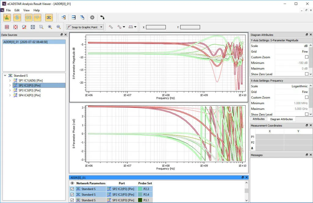
Simulation accuracy demands correlation with physical measurements. Time-domain reflectometry (TDR) visualizes impedance profiles along traces, identifying discontinuities quickly and robustly. Vector network analyzers (VNAs) provide frequency-domain S-parameters up to high GHz ranges for detailed loss and reflection analysis.
Best practices include building test structures on panels, using consistent probing techniques, and applying correction factors for unmodeled effects like surface roughness. Excellent correlation between TDR/TDT and VNA-extracted S-parameters is achievable when setups align. Calibrate material libraries iteratively to align models with fabricated boards, refining predictions for future designs.
Real-World Applications and Case Insights
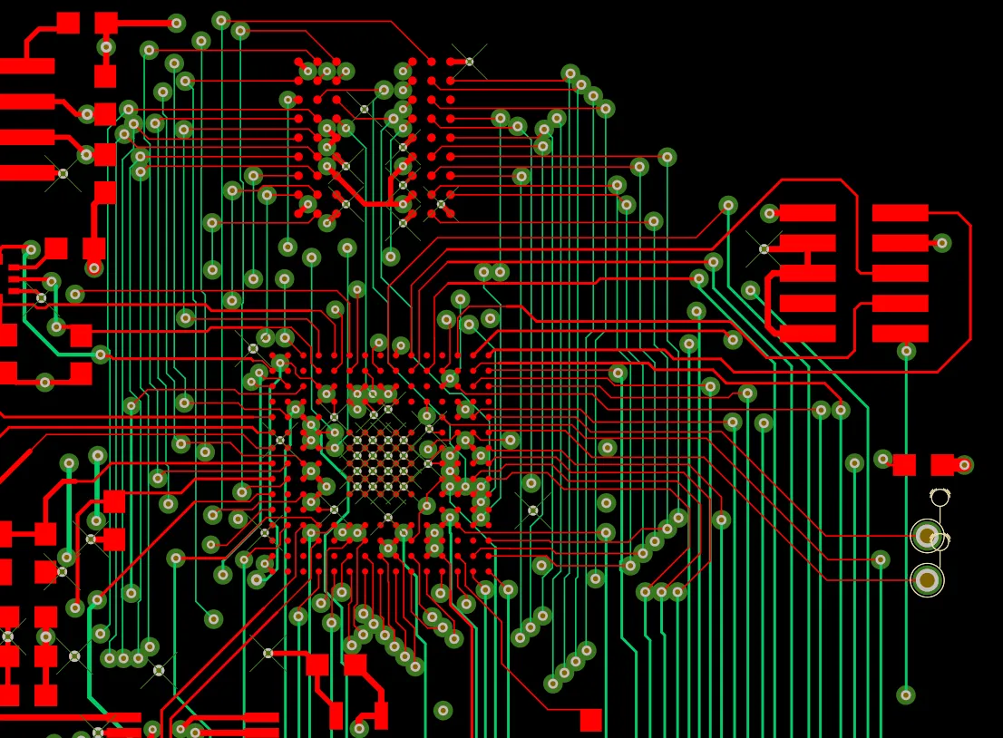
Consider a 16-layer backplane for 112 Gbps PAM4 signaling, where tight impedance tolerances demand advanced modeling. Initial 2D calculations suggested 80-micron traces, but finite element analysis revealed 15% deviation due to coupling. Refining the stackup with low-loss dielectrics stabilized Z0 at 85 ohms differential. Electromagnetic simulation predicted via crosstalk below -40 dB, confirmed post-fab. Signal integrity analysis chained with transmitter models yielded 30% eye opening improvement. Such cases highlight simulation's role in pushing bandwidth limits. Similar challenges in via effects and differential pairs are addressed in via placement for differential pairs.
Conclusion
Advanced techniques in PCB impedance control through simulation and modeling provide electric engineers with powerful tools to conquer high-speed design challenges. From fundamental principles to finite element analysis and full-wave electromagnetic simulation, these methods ensure predictable performance. Integrating PCB simulation software and signal integrity analysis into workflows aligns designs with manufacturing realities and standards. Best practices like iterative verification and tolerance analysis minimize risks. As frequencies rise, mastery of impedance modeling becomes a competitive edge, enabling reliable, high-performance electronics.
FAQs
Q1: What role does PCB simulation software play in impedance control?
A1: PCB simulation software performs rapid field solving to predict trace impedance based on stackup and geometry, enabling pre-layout adjustments. It supports parametric studies for tolerance analysis, crucial for signal integrity analysis. Electric engineers use it to verify 50-ohm or 100-ohm targets before routing. This reduces fabrication iterations and ensures compliance with design rules. Overall, it streamlines high-speed PCB development efficiently.
Q2: How does electromagnetic simulation improve impedance modeling accuracy?
A2: Electromagnetic simulation solves full 3D Maxwell's equations, capturing discontinuities like vias and bends that 2D models miss. It accounts for frequency-dependent effects such as skin effect and dielectric losses. Finite element analysis within these tools refines meshes for precise field distributions. Engineers gain insights into crosstalk and reflections for better impedance modeling. This leads to robust designs with validated signal integrity.
Q3: Why is finite element analysis essential for complex PCB structures?
A3: Finite element analysis discretizes irregular geometries into elements, solving for accurate capacitance and inductance. It handles multilayer coupling and embedded passives effectively. In signal integrity analysis, it extracts S-parameters for broadband validation. This method outperforms approximations in HDI boards with fine-pitch features. Engineers rely on it for confidence in high-frequency performance.
Q4: What are key steps in signal integrity analysis for impedance control?
A4: Begin with impedance extraction from layout, followed by channel simulation using TDR/eye diagrams. Assess reflections, loss, and jitter margins. Electromagnetic simulation verifies critical nets. Correlate with measurements for model calibration. This workflow ensures end-to-end integrity in high-speed PCBs.
References
IPC-2141 — Controlled Impedance Circuit Boards and High Speed Logic Design. IPC.
IPC-2221 — Generic Standard on Printed Board Design. IPC.
IPC-6012 — Qualification and Performance Specification for Rigid Printed Boards. IPC.


