Introduction
In PCB manufacturing, yield represents the percentage of boards that pass all quality checks without rework or scrap, directly impacting production costs and delivery timelines. Common PCB manufacturing errors and yield losses often stem from issues during fabrication and early assembly stages, leading to defects like warpage, delamination, and via failures. These problems not only increase scrap rates but also delay time-to-market for electronic products relied upon by electric engineers. Identifying these errors early through systematic inspection enables factories to implement corrective actions, boosting overall efficiency. This guide focuses on prevalent defects, their root causes, and practical resolution strategies aligned with industry standards. Electric engineers benefit from understanding these factory-driven insights to optimize designs and collaborate effectively with manufacturers.
Understanding PCB Yield and Why Manufacturing Errors Matter
PCB yield measures the ratio of functional boards to total produced, with high yields essential for cost-effective scaling in high-volume production. Low yields from manufacturing errors amplify expenses through material waste, labor for rework, and testing overheads. For instance, a 5 percent drop in yield on a mid-sized run can equate to significant financial losses, underscoring the need for proactive defect management. Electric engineers encounter these issues when boards fail reliability tests or assembly processes, tracing back to fabrication inconsistencies. Adhering to standards like IPC-6012 helps define performance qualifications that minimize such risks. Ultimately, mastering common PCB manufacturing errors and yield challenges ensures robust product lifecycles.
Common PCB Manufacturing Errors and Their Impact on Yield
Manufacturing processes involve multiple steps from lamination to drilling, etching, and plating, each prone to defects that compromise yield. Warpage tops the list, occurring when boards bow or twist beyond acceptable limits due to thermal stresses or material imbalances. Delamination follows, where layers separate, often from contamination or inadequate bonding. Via defects, such as plating voids or cracks, disrupt electrical connectivity and plague multilayer boards. Solder mask anomalies and drill breakout further erode yield by affecting surface finish and hole integrity. These errors collectively demand rigorous root cause analysis PCB defects to prevent recurrence.
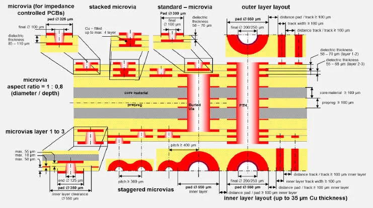
Warpage: Causes and Identification
Warpage arises primarily from asymmetric copper distribution, improper bake-out of laminates, or mismatched coefficients of thermal expansion between materials. During lamination or reflow, uneven heating exacerbates bowing, exceeding tolerances specified in IPC-A-600 for board flatness. Engineers identify it visually or with precision tools like dial gauges on bowed sections. Severe cases halt automated assembly lines as pick-and-place machines misalign components. Yield drops as warped boards fail coplanarity tests, requiring flattening or scrapping. For visual detection methods, explore our guide on How AOI Equipment Detects Common PCB Defects.
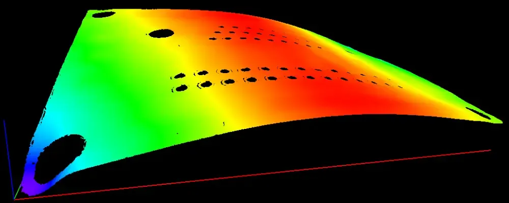
Early detection through post-lamination stress relief baking mitigates this, maintaining board planarity under operational temperatures.
Delamination: Layer Separation Challenges
Delamination manifests as blisters or full separation between copper and prepreg layers, triggered by moisture absorption, resin voids, or excessive drill heat. Contaminated surfaces from handling or poor panel cleaning accelerate this during multi-step pressing. Cross-section microscopy reveals the extent, showing adhesive failures at interfaces. Yield suffers as delaminated boards exhibit opens or shorts in testing. Factories align processes with IPC-6012 to qualify laminates against such failures under thermal cycling. Corrective measures include vacuum-assisted lamination to expel air pockets.
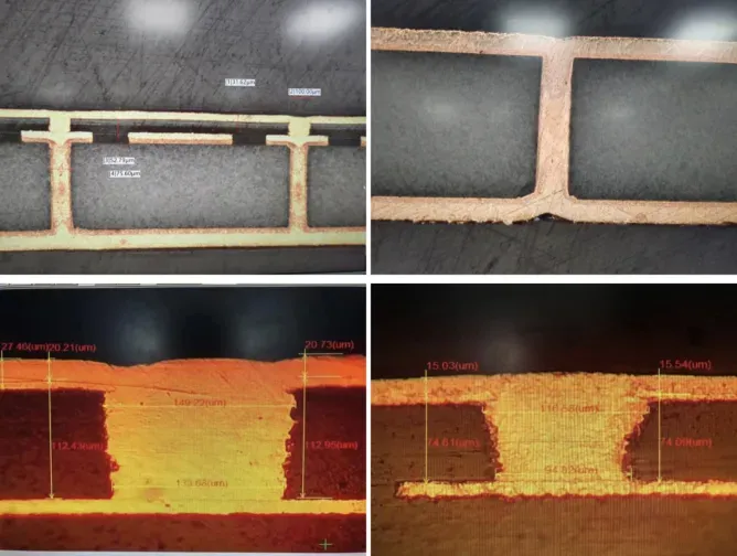
Via and Plating Defects: Connectivity Killers
Vias fail from barrel cracks, plating voids, or tenting issues during electroless or electrolytic plating processes. Root causes include over-etching, inadequate desmear, or current density variations in plating baths. X-ray inspection uncovers hidden voids that electrical tests miss initially. These defects slash yield by causing intermittent opens in high-density interconnects. Engineers performing root cause analysis PCB defects use dye-and-pull tests for adhesion verification. Optimizing sequential lamination reduces stress concentrations around vias.
Solder Mask and Surface Finish Problems
Solder mask defects like blisters, pinholes, or delamination occur from overexposure to UV or liquid photoimageable inconsistencies. Poor adhesion stems from plasma cleaning oversights or substrate contamination. These issues lead to PCB assembly yield problems by promoting bridging or exposed copper oxidation. Visual and automated optical inspection (AOI) flags non-conformances per acceptability criteria. Yield improves with precise exposure controls and post-cure verification. Surface finish anomalies, such as uneven HASL or ENIG, further complicate soldering reliability.
Drilling and Hole Wall Imperfections
Drill breakout or rough hole walls result from dull bits, improper feed rates, or entry-exit material mismatches. Excessive smear from high-speed drilling without adequate backing impairs plating adhesion. Microsection analysis confirms wall pull-away or cone-shaped breakouts. These manufacturing flaws directly lower yield through plating shorts or opens. Implementing peck drilling cycles and entry material selection enhances hole quality. Standards guide tolerance limits to sustain interconnect integrity.
Root Cause Analysis Techniques for PCB Defects
Root cause analysis PCB defects employs a structured approach starting with failure mode documentation and 5-Why interrogation. Visual and dimensional checks precede advanced methods like scanning electron microscopy (SEM) for contamination sources. X-ray and acoustic microscopy detect internal voids without destructive sampling. Cross-sectioning provides definitive evidence of layer interfaces or plating thickness. Thermal profiling correlates process parameters to stress-induced failures. Factories integrate these with statistical process control to trace variations back to equipment or materials.
For warpage, finite element modeling simulates stack-up responses, while dye penetrant tests highlight microcracks. Delamination probes moisture content via baking weight loss. Yield data logging across lots pinpoints supplier or batch issues. Collaborative reviews with design teams refine DFM rules. This methodical RCA elevates manufacturing maturity, targeting sub-1 percent defect rates. Integrate these techniques early with our Design for Yield: How DFM Principles Can Radically Improve PCB Manufacturing Success.
Best Practices to Minimize Errors and Boost Yield
Implement design for manufacturability (DFM) reviews early, balancing copper weights and specifying CTE-matched materials. Process controls like automated plating current monitoring prevent voids. Pre-baking panels removes moisture per JEDEC guidelines, averting popcorn effects in assembly. In-line AOI and flying probe testing catch defects pre-shipment. Operator training on handling per IPC standards reduces contamination. Statistical yield tracking via Cpk analysis drives continuous improvement. Learn SMT-specific yield strategies in Tackling SMT Assembly Challenges to Maximize PCB Yield.
Supplier qualification ensures laminate consistency, while panel size optimization aids handling. Post-etch rinse protocols eliminate residues affecting mask adhesion. These practices collectively address common PCB manufacturing errors and yield pitfalls, fostering reliable production.
Troubleshooting Step-by-Step Guide
Begin troubleshooting with yield data segregation by process step to isolate fabrication versus assembly faults. Conduct 100 percent visual inspection against IPC-A-600 criteria, photographing anomalies. Sample destructive analysis on failed lots reveals patterns like consistent via voids. Correlate with process logs for temperature spikes or chemical imbalances. Adjust parameters iteratively, validating with test coupons. Document findings in a Pareto chart to prioritize fixes, recirculating good panels where feasible.
For persistent PCB assembly yield problems, profile reflow ovens against component profiles. Moisture barrier bags protect boards during storage. Engineer-factory loops refine specs, closing the feedback cycle.
Conclusion
Addressing common PCB manufacturing errors and yield challenges requires vigilance across fabrication stages, from lamination to finishing. Warpage, delamination, via issues, and surface defects dominate losses, but root cause analysis PCB defects unlocks targeted resolutions. Leveraging standards like IPC-6012 and IPC-A-600 ensures consistent quality benchmarks. Best practices in DFM, process controls, and inspection yield sustainable improvements. Electric engineers partnering with informed factories achieve higher reliability and cost savings. Proactive management transforms troublesome boards into high-yield successes.
FAQs
Q1: What are the most common PCB manufacturing errors and yield impacts?
A1: Warpage, delamination, and via plating voids rank highest, each reducing first-pass yield by disrupting assembly alignment or electrical performance. Factories mitigate these through stack-up symmetry and plating optimizations. Yield tracking identifies trends early, preventing batch-wide losses. Standards like IPC-A-600 define acceptable limits for quick triage.
Q2: How does root cause analysis help with PCB defects?
A2: Root cause analysis PCB defects uses tools like X-ray and cross-sectioning to pinpoint sources such as contamination or process excursions. It shifts focus from symptoms to preventives, like enhanced cleaning cycles. Electric engineers apply 5-Why methods for design inputs. Results inform supplier audits and process tweaks for yield gains.
Q3: What causes PCB assembly yield problems during manufacturing?
A3: Surface defects like solder mask pinholes or exposed copper from etch residues lead to bridging or poor wetting in reflow. Warped boards misalign components, amplifying tombstoning. Pre-assembly inspections per IPC standards catch these. Optimizing stencils and paste volumes resolves many issues upstream.
Q4: How can factories improve PCB manufacturing yield overall?
A4: Adopt in-line metrology, DFM collaboration, and statistical controls to monitor key parameters. JEDEC moisture handling prevents hidden failures. Training and equipment PM sustain consistency. Yield mapping correlates defects to steps, enabling targeted SPC adjustments for long-term stability.
References
IPC-6012E — Qualification and Performance Specification for Rigid Printed Boards. IPC, 2017
IPC-A-600K — Acceptability of Printed Boards. IPC, 2020
JEDEC J-STD-020E — Moisture/Reflow Sensitivity Classification. JEDEC, 2014