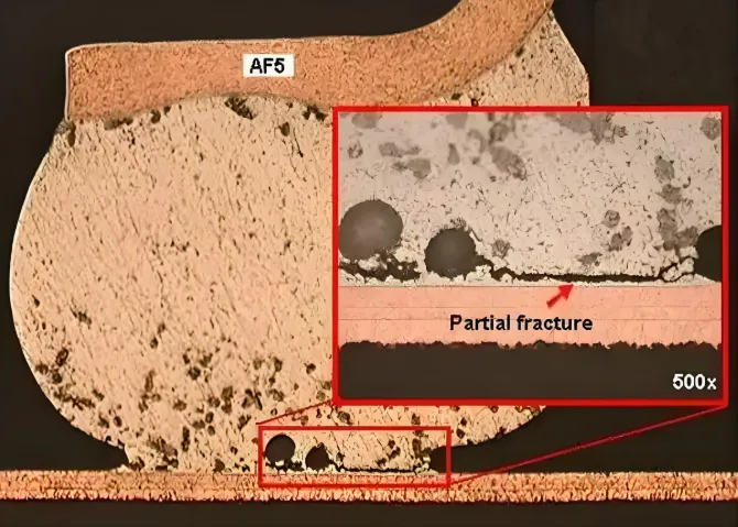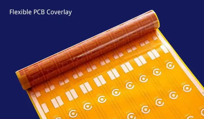
What Happens If FPC Coverlay Opening Is Too Large?
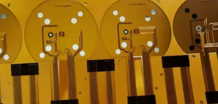
Oversized FPC coverlay openings leave copper exposed to oxidation, reduce pad support, and raise flex fatigue risk. Practical guidelines for correct flexible PCB coverlay opening size and clearance.
Printed circuit boards (PCBs) form the backbone of modern electronics, serving as the essential platform for connecting components in devices ranging from smartphones to industrial machinery. In our PCB Types category, we delve into the diverse array of PCB designs and configurations available today, exploring how each type addresses specific engineering challenges and performance needs. Whether you are a hobbyist building a prototype or an engineer optimizing for high-frequency applications, understanding these variations is crucial for selecting the right board for your project. The scope of PCB Types encompasses everything from single-layer boards ideal for simple circuits to complex multilayer designs that support advanced signal integrity and thermal management. We cover rigid, flexible, and rigid-flex PCBs, along with specialized options like high-density interconnect (HDI) and metal-core boards used in power electronics. This category highlights the practical value of these choices, such as enhancing durability in automotive systems or enabling compact designs in wearable technology. By examining real-world applications, from consumer gadgets to aerospace equipment, readers gain insights into how PCB selection influences reliability, cost efficiency, and overall system performance. Our articles provide comprehensive guides on evaluating PCB types for different environments, tutorials on assembly techniques, and best practices for material selection to avoid common pitfalls. We also share expert insights into emerging trends, such as eco-friendly substrates and advancements in 5G-compatible boards. These resources equip professionals and enthusiasts with the knowledge to innovate and troubleshoot effectively. As you navigate through the posts in this category, you will discover strategies to apply in your own designs, fostering a deeper appreciation for the technical nuances that drive electronic innovation.
Oversized FPC coverlay openings leave copper exposed to oxidation, reduce pad support, and raise flex fatigue risk. Practical guidelines for correct flexible PCB coverlay opening size and clearance.
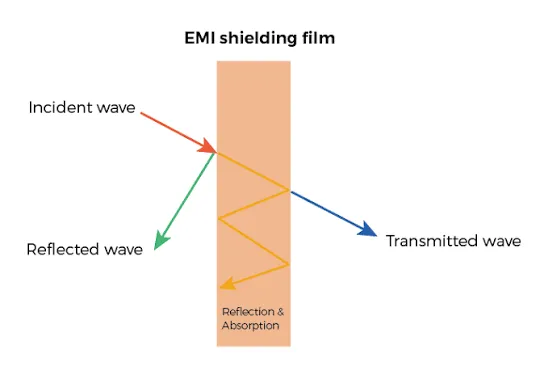
FPC EMI shielding changes the reference plane, impedance, and return path. Practical layout rules for film vs copper shields that protect high-speed signal integrity without creating new discontinuities.
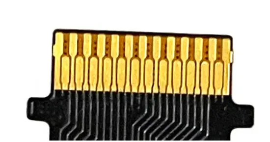
FPC gold finger wear and flexible PCB connector failure are driven by hard gold thickness and friction in production. See how factories set plating limits, control nickel underlayer, and match surface finish to mating cycles to stop early wear.
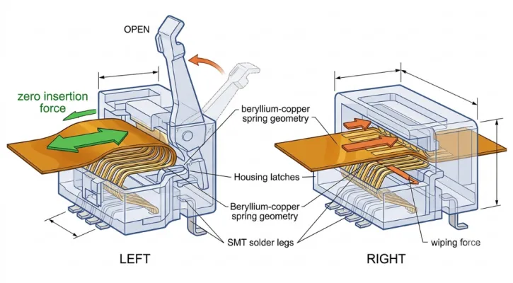
Practical FPC connector design rules for ZIF flexible PCBs: gold finger length/width/thickness, coverlay setback, stiffener placement, and mating-cycle plating to prevent insertion failures and intermittent contact.
FPC short circuit between traces usually comes from insufficient finished spacing after etch undercut, residual copper, or conductive debris. High-density layouts shrink the process window. Practical spacing rules and etch/AOI limits that prevent flexible PCB trace shorts.
FPC open circuits after manufacturing usually stem from over-etched thin traces, copper cracks in bend zones, or missed latent opens. Practical design and process fixes that stop flexible PCB trace breaks.
FPC electrical test failures (open, short, resistance) usually trace to layout geometry, etch undercut, and coverlay registration. Practical DFM rules that cut flexible PCB open short failure rates.
2oz copper FPC trace width and 3oz flexible PCB designs struggle with fine pitch due to etch undercut and yield loss. See real factory limits, safe L/S rules, and when to choose thin vs heavy copper.
In real FPC production, stiffener holes are always opened larger than the drill holes to cover bonding offset and material shift. See the exact compensation used for FR4 and aluminium reinforcement.
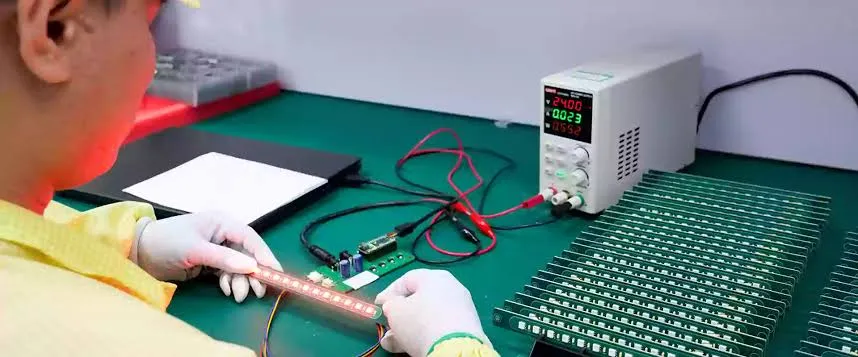
How factories actually run FPC testing methods and flexible PCB inspection before shipment: 100% electrical test, AOI for pattern/coverlay, visual checks, plus bend and thermal-shock sampling by application.
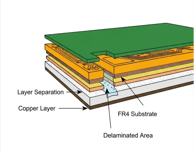
FPC delamination starts at the coverlay-adhesive-PI interface. See how factories control lamination, peel strength, contamination and DFM to stop flexible PCB layer separation before it hits yield and assembly.
FPC solder joint cracking after assembly usually comes from thermal mismatch, flex stress, and components placed too close to bend zones. See how factories control it in real production.