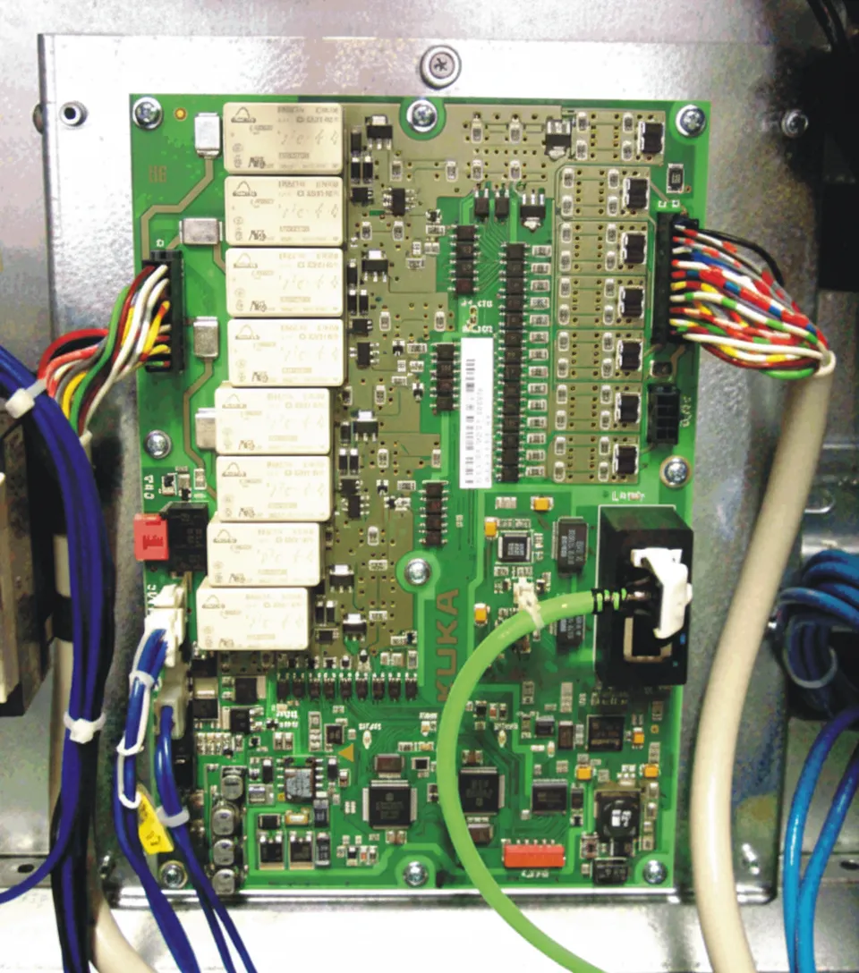
Artificial Intelligence continues to transform industries through advanced perception, decision-making, and automation. From robotics and autonomous vehicles to industrial control, medical devices, and consumer electronics, AI systems place unprecedented demands on the underlying hardware. At Aivon, we specialize in manufacturing high-performance PCBs that enable reliable, efficient, and scalable AI implementations through optimized power delivery, high-speed signal integrity, thermal management, and advanced fabrication techniques.
This article examines core AI principles, machine learning algorithms, neural network training, model development stages, and foundational software from a PCB engineering viewpoint.
Core Principles of Artificial Intelligence and PCB Hardware Requirements
AI systems replicate human-like intelligence using data-driven models rather than explicit programming. Key principles include learning from experience, pattern recognition, reasoning, and adaptation. Real-world applications span computer vision, natural language processing, predictive maintenance, and autonomous navigation.
PCB Design Implications:
- High Computational Load: AI workloads require powerful processors (GPUs, TPUs, NPUs) or FPGAs. PCBs must support high-density interconnect (HDI) with microvias, fine-pitch BGAs, and multi-layer stack-ups (8-20+ layers) to accommodate dense processing units.
- Data Throughput: High-bandwidth interfaces such as PCIe, MIPI, Ethernet, and DDR memory demand controlled impedance routing, length matching, and low-loss materials to maintain signal integrity at multi-gigabit speeds.
- Power Integrity: AI accelerators consume significant current with rapid transients. Dedicated power planes, multiple decoupling capacitor arrays, and low-noise voltage regulators (LDOs and DC-DC converters) are essential to prevent voltage droops that could corrupt computations.
Top Machine Learning Algorithms and Their Impact on PCB Architecture
Common machine learning algorithms vary significantly in computational complexity and memory requirements:
- Supervised Learning (Linear Regression, Logistic Regression, SVM, Decision Trees, Random Forests, KNN, Naive Bayes)
- Unsupervised Learning (K-Means, PCA, Autoencoders)
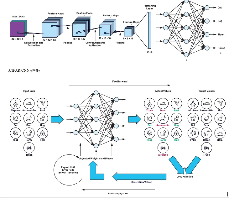
- Deep Learning (CNNs, RNNs/LSTMs, Transformers)
PCB Considerations:
- Algorithms like CNNs and Transformers involve massive parallel matrix operations. This drives the need for wide data buses and high memory bandwidth, requiring careful layer stack-up design with reference planes to minimize crosstalk and EMI.
- Training and inference phases generate substantial heat. Solutions include thicker copper (2oz-4oz), thermal vias arrays, metal-core PCBs (MCPCB), or high-Tg laminates for sustained thermal stability.
- Edge AI deployments in robotics or industrial systems favor compact designs where power efficiency directly affects battery life and system reliability.
Training Neural Networks: Computational and Hardware Challenges
Neural network training involves forward propagation, loss calculation, backpropagation, and weight optimization using large datasets. This process is highly parallel and memory-intensive, often requiring thousands of epochs with floating-point operations.
Key PCB Engineering Challenges:
- Memory Bandwidth: Large models need high-speed DDR4/DDR5 or HBM interfaces. PCB layout must prioritize short, matched traces and proper termination to avoid signal degradation.
- Power Delivery Networks (PDN): Peak currents during training can exceed hundreds of amperes. Optimized PDN design with plane segmentation, via stitching, and efficient voltage regulation prevents hotspots and ensures stable operation.
- Thermal Management: Training generates concentrated heat on AI chips. Advanced techniques such as embedded copper coins, heavy copper planes, and strategic component placement help dissipate heat while protecting sensitive analog or sensor interfaces from thermal drift.
- Reliability: Repeated high-load operation increases risk of solder joint fatigue and material degradation. Robust manufacturing processes - including via filling, back-drilling, and enhanced solder mask - improve long-term reliability in AI hardware.
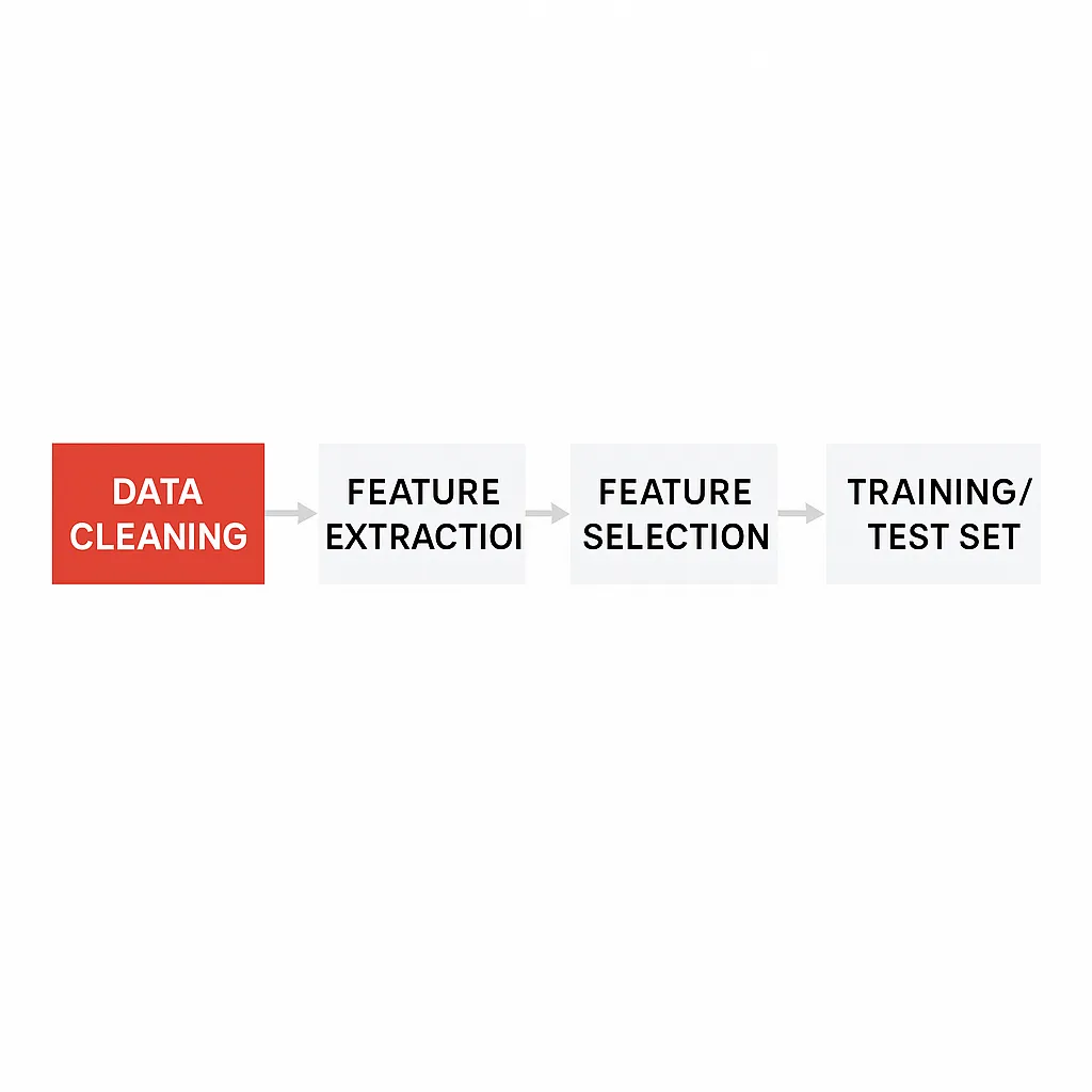
Five Stages of AI Model Development and PCB Support
Successful AI deployment typically follows these stages: Problem Definition, Data Collection & Preparation, Model Selection & Training, Evaluation & Optimization, and Deployment & Monitoring.
PCB-Level Considerations Across Stages:
- Data Preparation & Training: Requires high-throughput I/O and storage interfaces. PCBs need robust high-speed connectors and routing for SSDs or network interfaces.
- Evaluation & Optimization: Iterative testing stresses power and thermal systems. Designs must maintain performance consistency across temperature variations.
- Deployment: Edge inference favors compact, low-power boards. Techniques like model quantization reduce computational load, allowing smaller form factors with HDI technology and optimized power domains.
- Monitoring: Real-time inference monitoring benefits from dedicated diagnostic traces and isolated sensor interfaces on the PCB.
Fundamentals and Types of AI Foundation Software in Hardware Context
AI foundation software includes frameworks (TensorFlow, PyTorch, ONNX), libraries for model optimization, and runtime environments for inference. These tools abstract complexity but still expose hardware constraints through acceleration backends.
Hardware Acceleration Strategies:
- Heterogeneous Computing: Combining CPUs, GPUs, and NPUs requires sophisticated PCB routing for high-speed inter-chip communication with minimal latency.
- Quantization and Pruning: Software techniques that reduce model size enable lighter PCB implementations with fewer layers and lower power budgets.
- Real-Time Inference: Low-latency requirements in robotics or automotive applications demand deterministic timing, achieved through precise clock distribution, ground plane integrity, and EMI shielding on the PCB.
Advanced PCB Manufacturing Strategies for AI Applications
To support modern AI systems effectively, consider these critical manufacturing aspects:
- Stack-Up Optimization: Balanced constructions with multiple ground and power planes for superior EMI/EMC performance and signal integrity.
- Material Selection: Low-loss dielectrics (e.g., Rogers or high-performance FR4 variants) for RF/high-speed sections; high-Tg materials for thermal resilience.
- Fabrication Techniques: Precision laser drilling for microvias, impedance control testing, and via-in-pad designs for dense AI modules.
- Thermal Solutions: Integrated heat spreaders, thermal via farms, and copper balancing to manage hotspots from AI accelerators.
- Cross-Industry Applications: Automotive ADAS, industrial predictive maintenance, medical imaging, and consumer smart devices all benefit from these robust PCB foundations.
AI continues to push the boundaries of electronics hardware. By addressing the specific demands of machine learning algorithms, neural network training, and inference workloads at the PCB level, engineers can achieve higher performance, better efficiency, and greater reliability.
At Aivon, our expertise in advanced PCB design and manufacturing helps translate complex AI requirements into production-ready boards that perform consistently across demanding environments. Whether developing edge AI solutions or high-performance computing platforms, partnering early with an experienced manufacturer ensures optimal results from prototype to volume production.