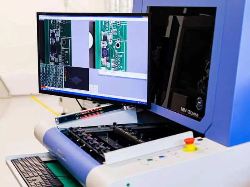
PCB Defects
Printed circuit boards (PCBs) are the backbone of modern electronics, but defects can compromise their performance, reliability, and safety. The PCB Defects tag on this blog gathers in-depth resources focused on identifying, analyzing, and resolving common issues that arise during design, manufacturing, and assembly processes. Whether you are a seasoned engineer troubleshooting production failures or a hobbyist diagnosing faults in a prototype, understanding these defects is essential for maintaining high-quality outcomes and minimizing costly rework. Common PCB defects include soldering problems like bridging or cold joints, trace discontinuities from etching errors, and component misalignment due to improper placement. Environmental factors such as humidity or thermal stress can also lead to delamination or warping, while design flaws might cause signal integrity issues like crosstalk. By exploring the articles under this tag, you gain practical knowledge on visual inspection techniques, such as using magnification tools or automated optical inspection (AOI) systems, to spot these issues early. Best practices emphasize preventive measures, including selecting appropriate materials, adhering to IPC standards for fabrication, and implementing robust quality control protocols during assembly. For those involved in PCB manufacturing, the tag offers actionable insights into root cause analysis methods like failure mode and effects analysis (FMEA), which help pinpoint recurring defects and streamline processes. Repair strategies, from simple reflow soldering to advanced rework stations, are covered to extend board lifespan without full replacement. This collection equips you with the tools to enhance yield rates, reduce downtime, and ensure compliance with industry regulations. As you delve into specific case studies and tutorials here, you will find tailored solutions that address real-world challenges, fostering better decision-making in your electronics projects.
Technical Articles
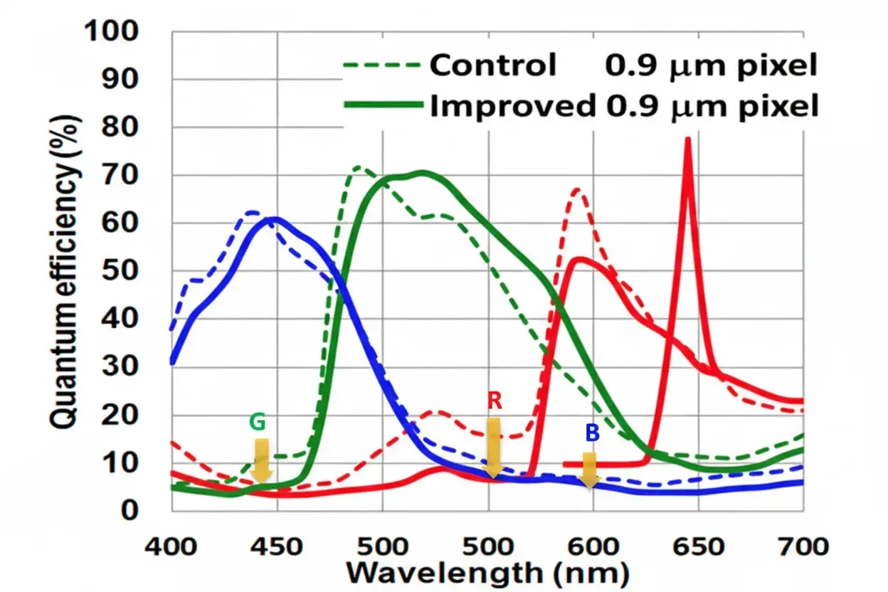
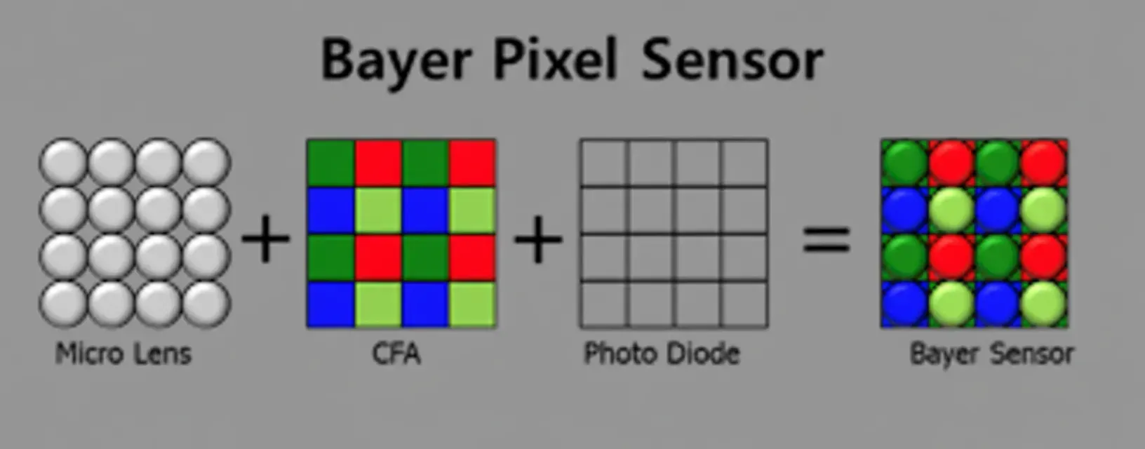
Quantum Efficiency Spectrum of CMOS Image Sensors
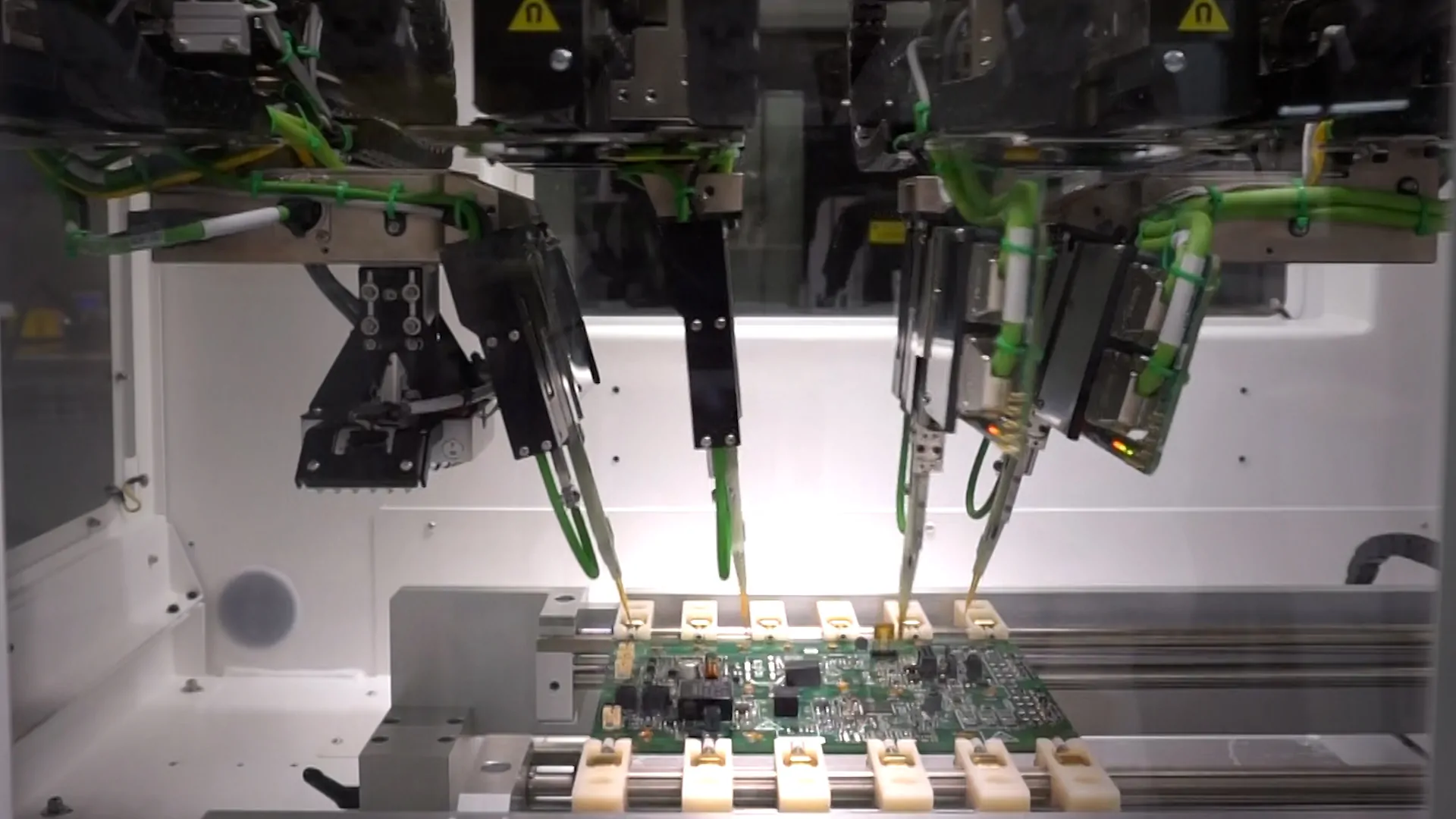
Boosting PCB Reliability: How Flying Probe Testing Minimizes Manufacturing Defects
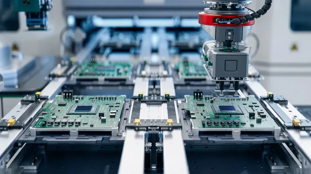
Optimizing DFM for High Volume PCB Manufacturing: A Comprehensive Guide
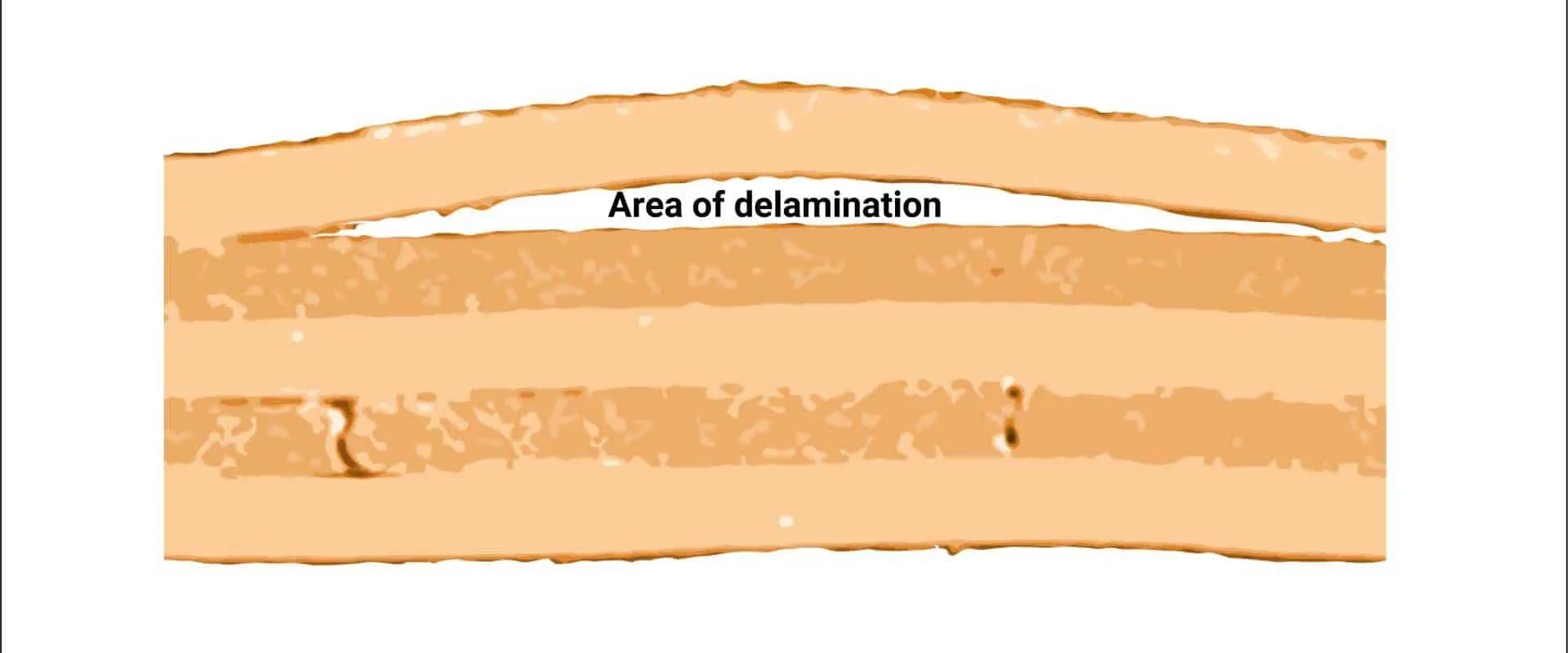
Overcoming PCB Manufacturing Challenges: Solutions for Common Defects and Production Issues
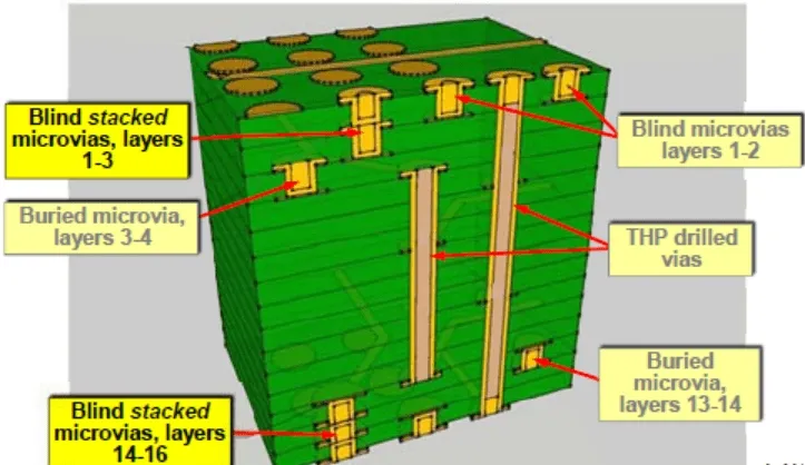
Troubleshooting Stacked Via Problems: A Practical Guide
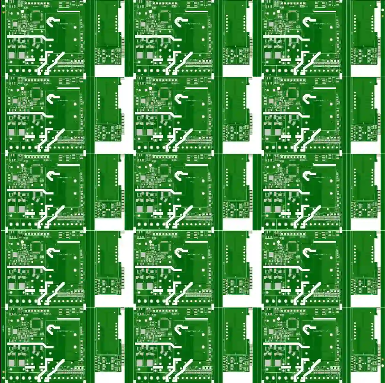
2-Layer FR-4 PCB Engineering Case: Copper-to-Edge Clearance, Asymmetric Via Pads, and Outline Data Issues

How to Fix Via Tenting, Non-Plated Holes, and Silkscreen Issues in 6-Layer PCB CAM Review
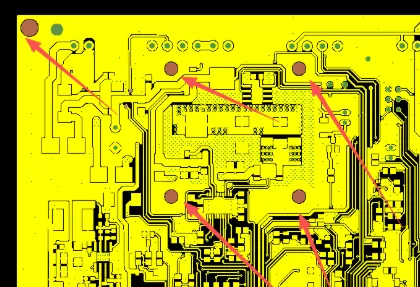
How to Fix 2 Layer FR4 PCB Design Errors During CAM Review
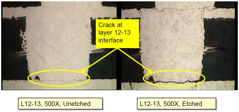
Why HDI Microvias Fail During Production
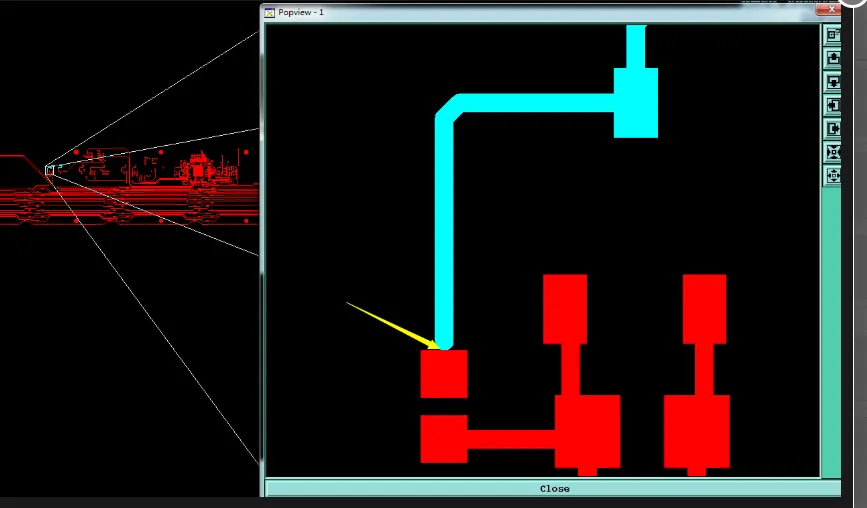
Avoid 4 Layer FR4 PCB Silkscreen and Solder Mask Production Errors
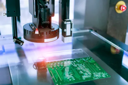
How AOI Equipment Detects Common PCB Defects: A Visual Guide
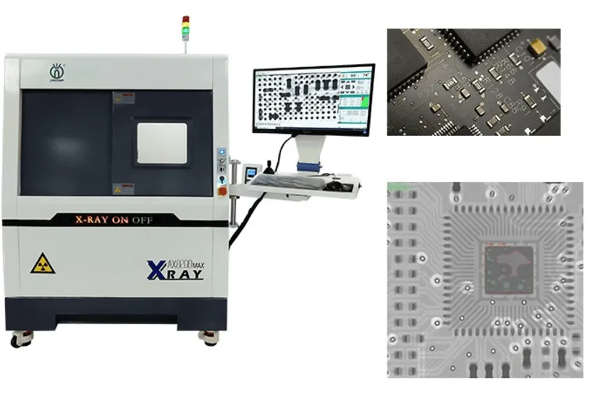
From Voids to Misalignments: A Complete Guide to PCB X Ray Inspection
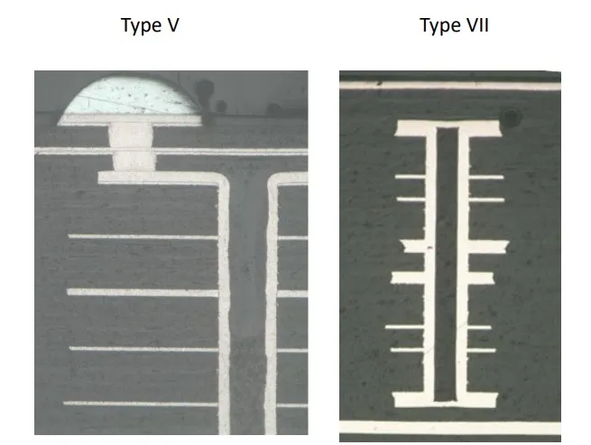
Troubleshooting Via Filling Defects: Identifying and Resolving Common Issues
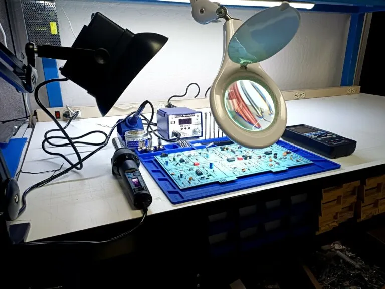
PCB Quality Control for Beginners: A Hobbyist's Guide
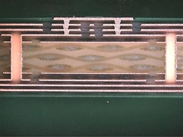
Delamination in PCB Lamination: Causes, Detection, and Prevention
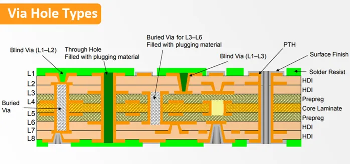
Troubleshooting Challenges in Blind and Buried Via PCB Manufacturing
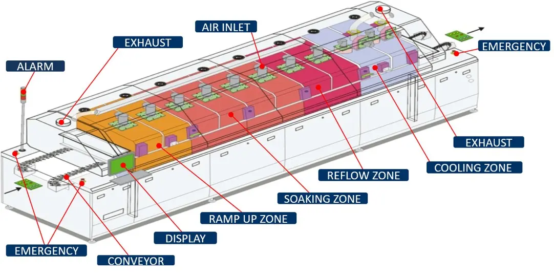
High Tg PCB Assembly: Best Practices for High Temperature Soldering
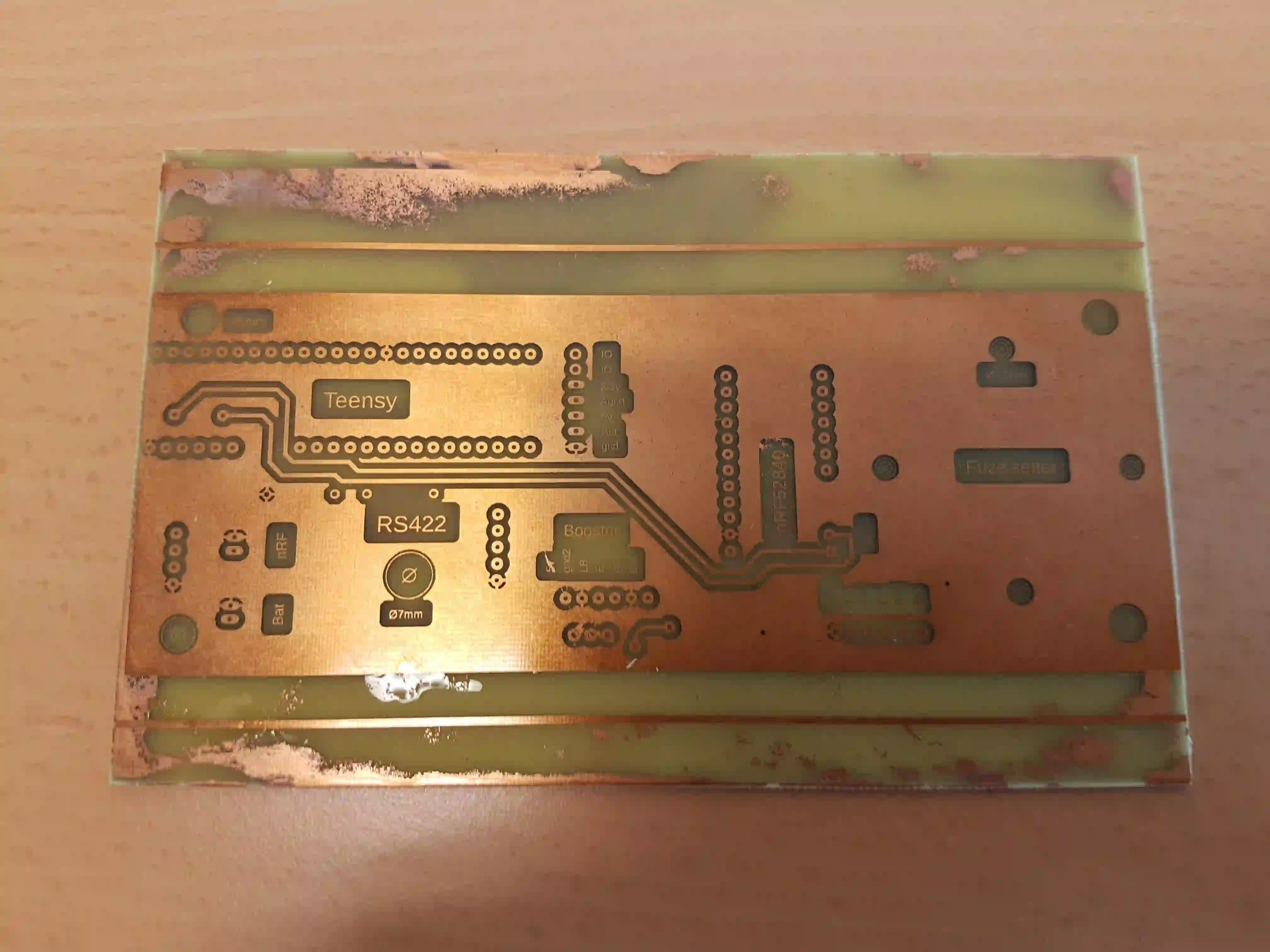
Aluminum PCB Manufacturing Defects: Identification, Prevention, and Solutions