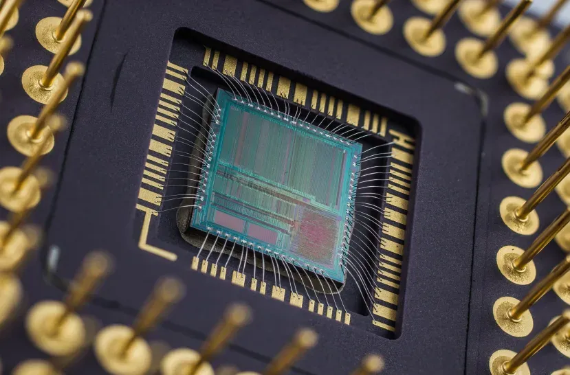
PCB Miniaturization
PCB miniaturization represents a critical advancement in electronics design, enabling the development of compact, high-performance devices that fit into increasingly smaller form factors. This tag explores the strategies, technologies, and challenges involved in reducing the size of printed circuit boards while maintaining functionality, reliability, and efficiency. For engineers, designers, and manufacturers searching for ways to optimize space in applications like wearables, IoT sensors, medical implants, and consumer gadgets, understanding PCB miniaturization is essential to meet demands for portability and integration without compromising performance. Key aspects covered under the PCB Miniaturization tag include advanced layout techniques such as high-density interconnect (HDI) boards, microvias, and buried vias, which allow for denser component placement and shorter signal paths. Practical applications highlight how selecting smaller components, like chip-scale packages and embedded passives, can significantly shrink board footprints while improving signal integrity and thermal management. Best practices emphasize iterative design processes, including simulation tools to predict electromagnetic interference and heat dissipation in miniaturized layouts, ensuring robust outcomes in real-world scenarios. Readers interested in overcoming common hurdles, such as manufacturing tolerances or cost implications, will find valuable insights into material choices, like flexible substrates or rigid-flex hybrids, that facilitate miniaturization. By delving into these topics, professionals can apply proven methods to innovate in competitive markets, from prototyping compact prototypes to scaling production for mass-market devices. The articles linked here provide in-depth guidance on implementing these techniques, helping you refine your designs for optimal results.
Video Guide
No videos found for this tag.
Technical Articles
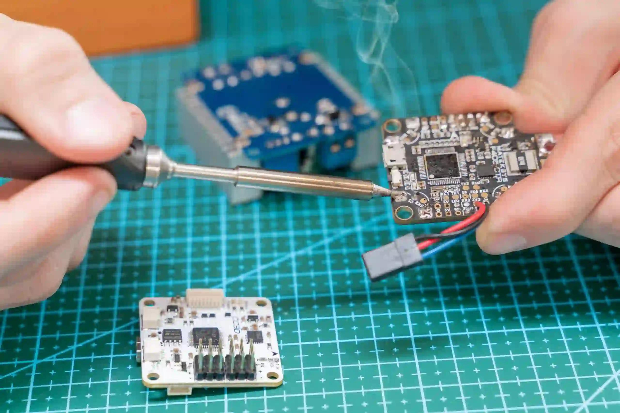
ICT in the Age of Miniaturization: Testing Micro Components on PCBs
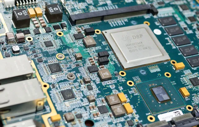
The Role of HDI PCBs in Telecommunication Base Stations: Benefits and Design Considerations
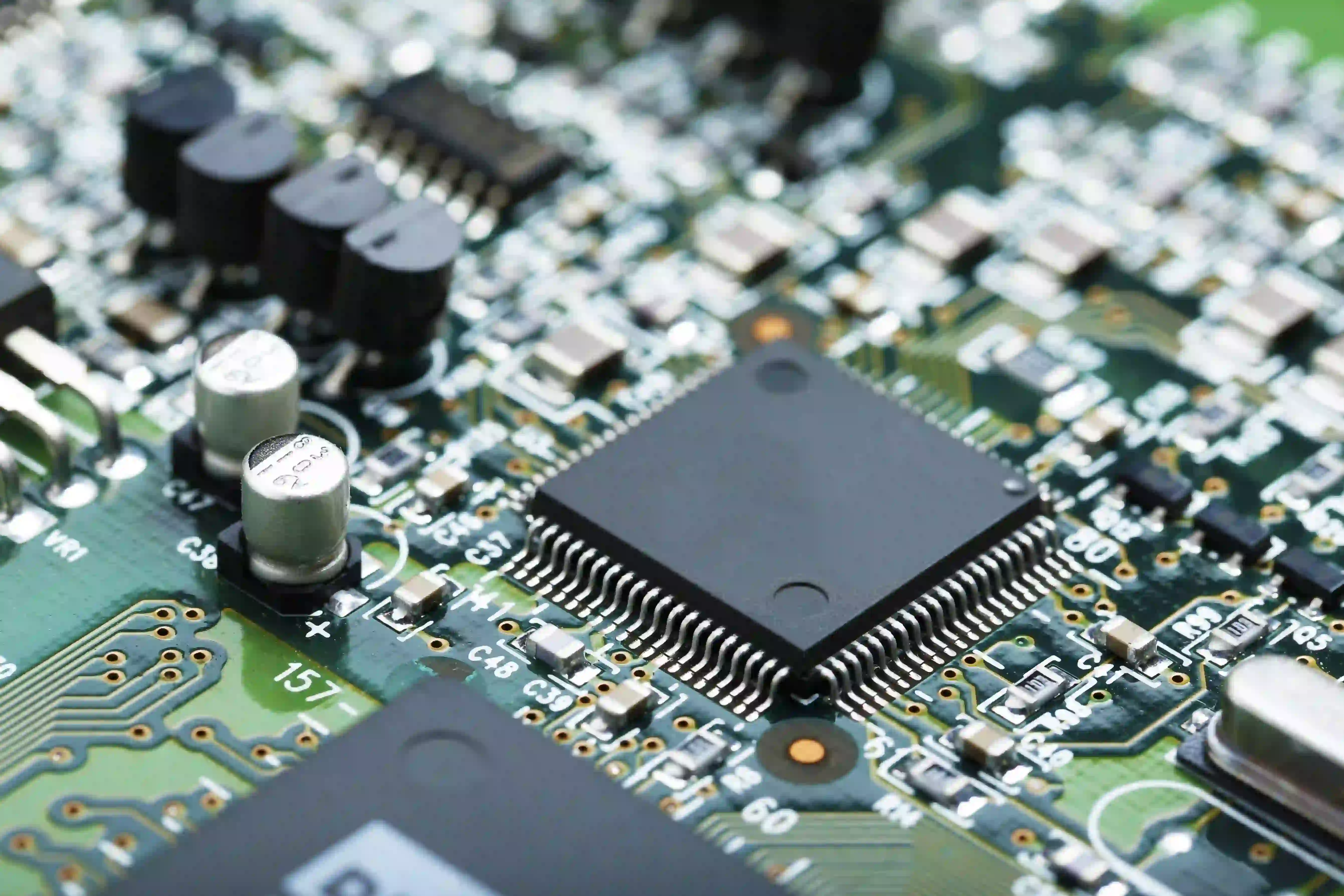
How Stacked Vias Revolutionize PCB Miniaturization
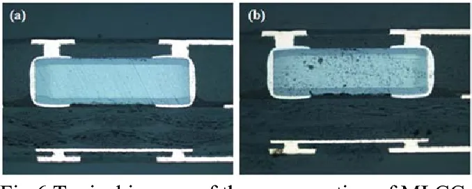
Embedded Components in Flexible Circuits: Design Considerations and Applications
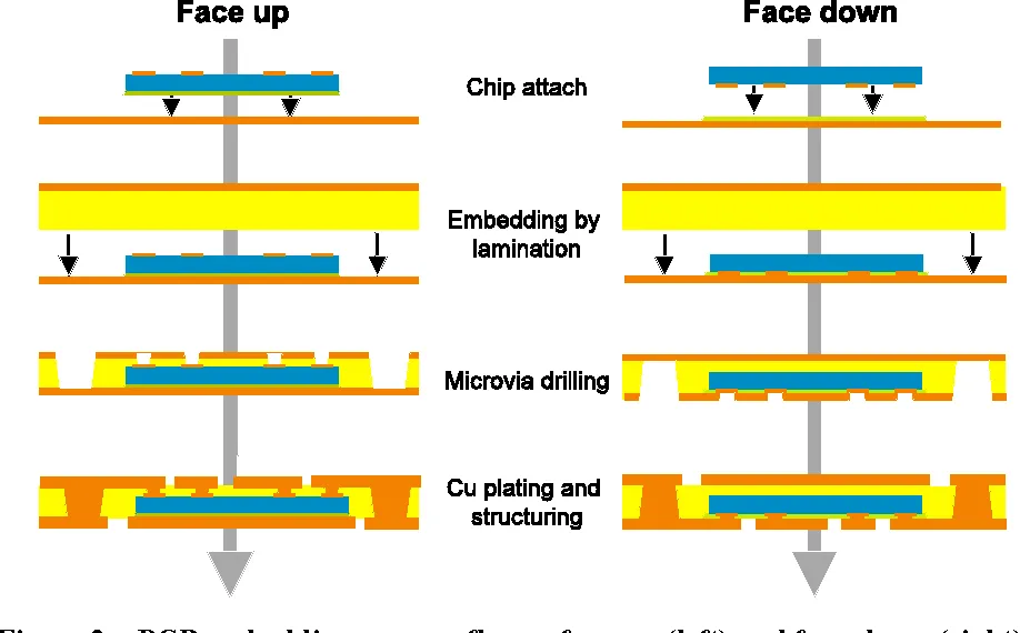
Beyond SMT: The Benefits of Embedding ICs Directly into Your PCB
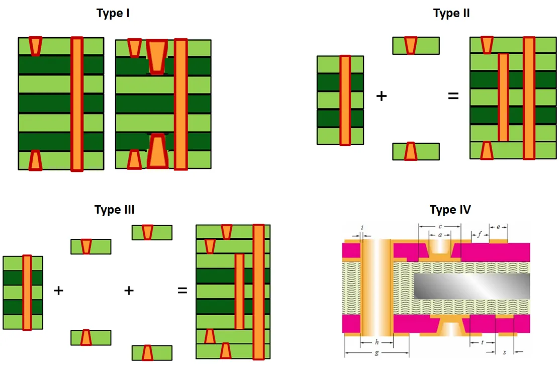
The Future of HDI PCBs: Trends in Miniaturization, Materials, and Manufacturing
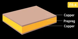
Ultra Thin FR 4 PCBs: Applications and Manufacturing Challenges
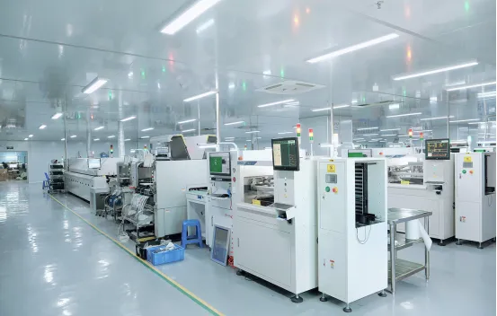
Component Alignment Testing: Ensuring Reliability in High Density PCBs
Get in Touch
Send Message
- Products & Service
- Company
- About AIVON
- Contact
- News
- Blog
- Certification
-


- Payment
-


2026 AIVON.COM All Rights Reserved