Introduction
In modern electronics, particularly in new energy applications, automotive systems, and high-performance industrial equipment, delivering clean and stable power is critical. Two closely related but distinct disciplines - Power Integrity (PI) and Power Electronics - play essential roles. While power electronics focuses on the design of power conversion circuits, power integrity ensures that this power is delivered effectively across the PCB to sensitive loads.
At Aivon, as specialists in PCB manufacturing and advanced electronics engineering, we frequently help clients optimize both aspects through intelligent PCB design, material selection, and layout strategies. This guide explains the differences, overlaps, and practical PCB-level implementation strategies for achieving excellent power delivery.
Understanding Power Integrity (PI) in PCB Context
Power Integrity refers to the ability of the Power Delivery Network (PDN) to provide stable voltage and current to all components with minimal noise and distortion. On a PCB, this involves everything from power planes and decoupling capacitors to trace routing and via design.
DC IR Drop and Current Handling
Ensuring sufficient copper thickness, plane continuity, and via arrays to minimize voltage drop under high current. In high-power new energy applications, inadequate copper weight or poor plane partitioning can lead to significant voltage sag.
AC Impedance and Decoupling
Maintaining low PDN impedance across a wide frequency range. This requires strategic placement of decoupling capacitors - combining bulk, mid-range, and high-frequency ceramics - with optimized via placement to reduce loop inductance.
Transient Response
Handling fast current demands (di/dt) from processors, FPGAs, or power switches without excessive voltage droop. Close proximity of capacitors to power pins and proper stack-up design (tight power-ground plane coupling) are essential.
Effective PI design heavily depends on PCB stack-up configuration, copper thickness (often 2oz or higher for power layers), and material selection (low-loss dielectrics for high-frequency performance).
Power Electronics: The Source Perspective
Power Electronics deals with the conversion, control, and regulation of electrical power - typically through switching converters (buck, boost, LLC, flyback, etc.). Key concerns include conversion efficiency, output ripple, load regulation, and EMI generation.
Common challenges in power electronics that directly impact PCB performance:
- Switching Noise and Ringing: High dv/dt and di/dt from MOSFETs create significant EMI.
- Output Ripple: Residual AC components on DC rails that can propagate through the PDN.
- Thermal Management: Heat generated by power devices must be dissipated effectively through the PCB.
From a PCB manufacturing viewpoint, power electronics circuits demand careful consideration of component placement, thermal vias, copper pours, and isolation between noisy switching sections and sensitive analog/digital domains.
Key Differences: Power Integrity vs Power Electronics
| Aspect | Power Electronics | Power Integrity (PCB Focus) |
|---|---|---|
| Primary Domain | Power conversion circuits and modules | Power delivery across PCB to loads |
| Main Metrics | Efficiency, ripple, stability, EMI | PDN impedance, IR drop, transient response |
| Tools | SPICE, circuit simulation | EM solvers (PIPro), full-wave analysis |
| PCB Impact | Generates noise sources | Manages noise propagation and delivery |
| Typical Concerns | Topology selection, control loops | Decoupling, plane design, stack-up |
Power electronics designs the "engine," while power integrity ensures the "fuel lines" deliver power cleanly.
PCB Design Strategies for Superior Power Integrity
1. Stack-up and Plane Design
Use tightly coupled power-ground plane pairs (<= 5-10 mil separation) to create distributed capacitance. For high-current applications, employ thicker copper (2oz-4oz) on power layers. Avoid irregular power plane shapes that create resonances.
2. Decoupling and Capacitor Strategies
- Place smallest value capacitors closest to IC power pins.
- Use parallel combinations (e.g., 100x ratio rule) for broad frequency coverage.
- Minimize via inductance through multiple vias per capacitor and optimized land patterns.
- Consider embedded capacitors or interposer techniques for ultra-high-frequency designs.
3. Ripple Measurement and Suppression on PCB
Ripple originates from switching action and insufficient filtering. On the PCB:
- Implement multi-stage LC filtering.
- Use ferrite beads and localized decoupling.
- Measure ripple with proper probing techniques (short ground loops, 20MHz bandwidth limit).
- Add snubber circuits to dampen ringing.
4. EMI Mitigation Using Snubbers and Layout
RCD snubber circuits are highly effective for absorbing energy from MOSFET switching and diode reverse recovery:
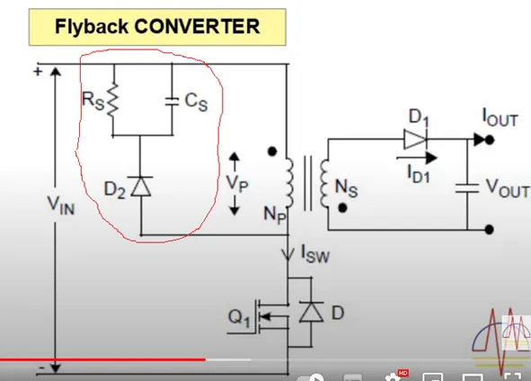
- Place RCD networks physically close to switching devices to minimize loop area.
- Combine with ferrite beads on rectifier diodes.
- Use ground stitching vias and proper partitioning between power and signal sections.
5. Thermal and High-Current Considerations
- Deploy thermal vias under power components.
- Calculate trace widths and copper thickness based on current density.
- Consider heavy copper PCBs or coin insertion for extreme power applications.
Common MOSFET Switching Circuits and PCB Implications
Power switching circuits (high-side/low-side, synchronous buck, etc.) require:
- Symmetrical layout for parallel MOSFETs.
- Kelvin sensing for accurate current measurement.
- Bidirectional current sensing techniques with low-side or inline shunts, considering trace resistance and thermal effects.
Overcurrent protection mechanisms should be implemented with fast-response circuits and proper PCB trace routing to avoid inductive spikes.
Best Practices for New Energy and High-Reliability Applications
In EV chargers, energy storage systems, and solar inverters:
- Prioritize low-inductance PDN designs.
- Use high-Tg materials and controlled impedance where necessary.
- Implement comprehensive EMI/EMC design from the early layout stage.
- Validate designs with power integrity simulation before fabrication.
Conclusion
Power Integrity and Power Electronics are complementary disciplines. Excellent power electronics performance can be undermined by poor PCB-level power delivery - and vice versa. By treating the entire PDN as a critical system and making informed choices in stack-up, materials, decoupling, and EMI suppression, designers can achieve reliable, high-performance systems.
At Aivon, we support customers with advanced PCB manufacturing capabilities - including heavy copper, HDI, high-Tg materials, and precise impedance control - specifically optimized for demanding power applications.
Need help optimizing your next power electronics PCB design? Our engineering team is ready to assist with DFM reviews, material recommendations, and production of high-reliability boards.