Switch-mode power supplies (SMPS) dominate modern electronics due to their high efficiency, compact size, and excellent voltage regulation. From buck converters in consumer devices to LLC resonant topologies in high-power new energy systems, SMPS performance depends heavily on PCB design, layout, and manufacturing decisions.
At Aivon, we specialize in turning power electronics schematics into reliable, manufacturable PCBs. This guide merges best practices for SMPS design with a strong focus on PCB-centric considerations - stack-up, trace routing, thermal management, EMI control, and fabrication implications.
Understanding SMPS Topologies and Their PCB Implications
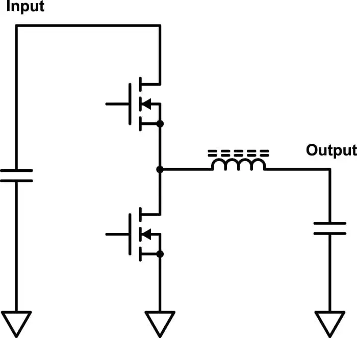
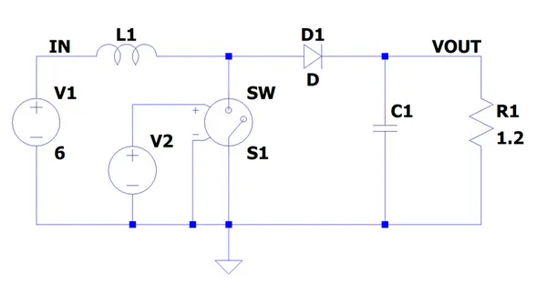
Common SMPS topologies include buck (step-down), boost (step-up), buck-boost, and resonant converters like LLC. The synchronous buck converter is particularly popular for its efficiency in point-of-load applications.
In a synchronous buck, two MOSFETs (high-side and low-side) switch alternately with an inductor and output capacitors. The switching node (SW) experiences high di/dt and dv/dt, making it the primary source of noise and EMI. Poor PCB layout here directly translates to increased ripple, EMI failures, and thermal hotspots.
Key PCB reframing:
- Minimize the high di/dt power loop area (input capacitor - high-side FET - SW - inductor - output capacitor - low-side FET).
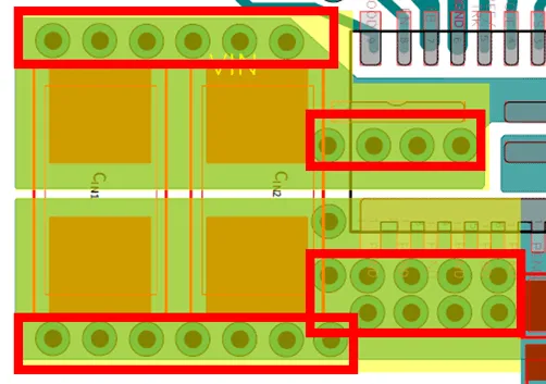
- Use proper via placement and copper thickness (2 oz or heavier for high-current paths) to handle peak currents without excessive voltage drop or heating.
LLC resonant converters suit high-power, high-efficiency applications (e.g., servers, EV chargers). Their zero-voltage switching reduces losses but demands precise magnetics and tight control of parasitic capacitances on the PCB.
Step-by-Step SMPS Design Process with PCB Focus
1. Define Specifications and Topology Selection
Start with input voltage range, output voltage/current, efficiency targets, size constraints, and environmental requirements (temperature, vibration). Choose topology based on step-up/down needs and power level. High switching frequencies (1-4 MHz+) allow smaller passives but increase PCB layout challenges.
2. Component Selection with Manufacturability in Mind
- Inductors: Balance saturation current, DCR, and core material. Smaller values at higher frequencies reduce size but demand low-parasitic PCB routing.
- Capacitors: Input ceramics for ripple current; output combinations for low ESR and adequate ripple suppression. Place multiple parallel capacitors to distribute current and heat.
- MOSFETs: Low Rds(on) for conduction losses; fast switching characteristics. Consider package thermal resistance and PCB copper for heat sinking.
- Controller ICs: Look for integrated features like adaptive dead-time, current sensing, and bootstrap circuitry. Bootstrap capacitors (C1) are critical for high-side gate drive in buck converters.
3. Schematic Design and Simulation
Use tools like LTspice for transient, stability, and efficiency analysis. Simulate worst-case conditions including component tolerances and PCB parasitics (inductance from traces/vias).
Critical PCB Layout Guidelines for Buck and SMPS Designs
PCB layout often determines whether a design succeeds or fails in EMI/EMC testing and thermal performance.
Power Loop Optimization
- Minimize the area of the hot loops (especially the switching loop). Place input capacitors as close as possible to VIN and PGND pins (< 40 mil recommended).
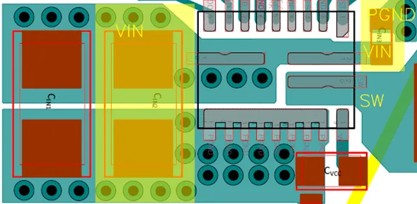
- Keep SW node traces short and wide but avoid unnecessary copper that increases capacitive coupling.
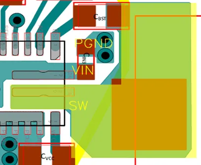
- Use multiple vias (6+ for VIN, 9+ for PGND) with adequate copper pour for current capacity and thermal relief. Follow IPC-2152 for trace width calculations.
Grounding Strategy
- Implement single-point grounding or careful star connections between AGND and PGND to prevent noise injection into sensitive feedback paths.
- Maximize ground plane area. Use solid copper pours on inner layers for high-current returns. Avoid ground loops that can act as antennas.
High-Frequency Considerations
- For regulators switching above 1 MHz, parasitic inductance and capacitance become dominant. Short traces, controlled impedance where needed, and strategic component placement reduce ringing and overshoot.
- Route sensitive signals (feedback, compensation) away from SW nodes and power loops. Use ground shielding when necessary.
Thermal Management on PCB
- High-current paths generate heat. Use heavy copper PCBs with wide traces, thermal vias under ICs and power components, and large copper planes.
- In multilayer boards, dedicate inner layers to power and ground planes for better heat spreading and lower impedance.
Component Placement Best Practices
- Place the power stage (FETs, inductor, input/output caps) first and compactly.
- Keep control circuitry somewhat separated but with short, clean connections.
- Position the entire SMPS block close to the load to minimize output voltage drop and improve transient response.
Advanced Techniques and Common Pitfalls
Reducing Inrush Current and Noise
Techniques include soft-start, NTC thermistors, or active inrush limiting. On the PCB, proper sequencing and decoupling help manage startup transients.
Adaptive Modes and Efficiency
Many modern controllers offer pulse-skipping or adaptive modes at light loads. PCB layout must support clean operation across modes without introducing instability.
High Step-Down Ratios and Ripple Control
For large Vin/Vout ratios, multi-phase or advanced topologies help. Output ripple issues often trace back to poor capacitor placement or excessive loop inductance.
Manufacturing and Reliability Considerations
- Choose stack-up carefully: more layers for complex power designs improve routing and EMI but increase cost.
- Specify controlled impedance if needed for high-speed control signals.
- Use high-Tg materials for thermal stability in power applications.
- Design for testability with probe points on critical nodes.
- Consider conformal coating or ruggedized construction for harsh environments (automotive, industrial).
Common failures include:
- Excessive EMI from large loop areas.
- Thermal runaway due to inadequate copper/vias.
- Oscillation from poor grounding or feedback routing.
- Component stress from parasitic inductance causing voltage spikes.
From Prototype to Production
After layout, fabricate prototypes and perform thorough testing: load transients, efficiency mapping, thermal imaging, and EMI pre-compliance scans. Iterate on the PCB as needed - minor copper pours or via additions often resolve issues.
Document layout rules and constraints for consistent production. At Aivon, we help optimize designs for DFM (design for manufacturability), ensuring high yield, controlled costs, and reliable supply chains.
Conclusion: PCB as the Foundation of SMPS Performance
Excellent SMPS design extends far beyond the schematic. The PCB is where electrical theory meets physical reality - parasitics, heat, and electromagnetic fields determine real-world success.
By prioritizing small power loops, strategic grounding, thermal design, and high-frequency considerations, engineers create robust power solutions for consumer electronics, automotive, telecom, industrial control, and new energy applications.
Partner with experienced PCB manufacturers like Aivon early in the design phase. Our expertise in power supply PCBs ensures your SMPS designs move smoothly from concept to high-volume production with superior reliability and performance. Contact our engineering team for design reviews, stack-up recommendations, or full turnkey PCB fabrication and assembly support.