Solar photovoltaic systems depend on efficient power electronics to maximize energy harvest, conversion, and system reliability. As solar cell technologies advance rapidly, the supporting printed circuit boards (PCBs) in inverters, MPPT controllers, optimizers, and monitoring systems must evolve to handle varying electrical characteristics, thermal profiles, and long-term stability demands. At Aivon, we specialize in high-performance PCBs tailored for next-generation solar applications.
Overview of Major Solar Cell Types
Solar cells are primarily classified into crystalline silicon, thin-film, and emerging third-generation technologies. Each type presents unique voltage, current, efficiency, and environmental resilience profiles that directly influence PCB design in downstream power electronics.
Crystalline Silicon Solar Cells remain the dominant technology, accounting for over 90% of the market. Within this category, key high-efficiency variants include:
- PERC (Passivated Emitter and Rear Cell)
- TOPCon (Tunnel Oxide Passivated Contact)
- HJT (Heterojunction Technology)
- IBC (Interdigitated Back Contact)
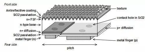
These architectures achieve module efficiencies of 22-26% in mass production, with TOPCon and HJT offering superior temperature coefficients and low-light performance. HJT cells, in particular, are frequently chosen as bottom cells in tandem structures due to their high open-circuit voltage.
Perovskite and Tandem Solar Cells
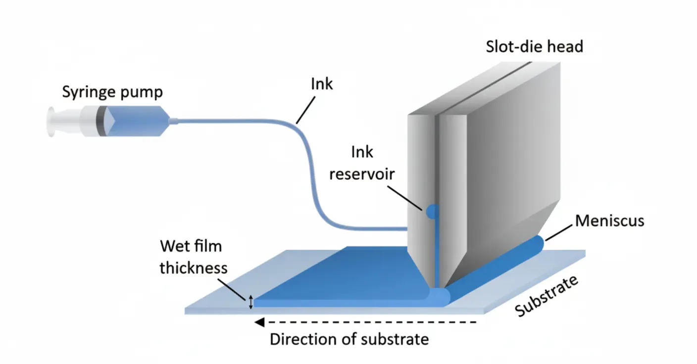
Perovskite solar cells have emerged as a promising thin-film technology with rapid efficiency gains, reaching over 25% in single-junction and 30%+ in perovskite-silicon tandem configurations. These cells are typically fabricated using scalable solution-based processes such as slot-die coating, followed by critical annealing steps to optimize crystal structure and performance.
Perovskite tandem cells combine a wide-bandgap perovskite top cell with a crystalline silicon bottom cell (often HJT). This architecture captures a broader solar spectrum while introducing new challenges:
- Different temperature-dependent behavior
- Faster initial degradation rates
- Unique I-V curve characteristics requiring adaptive power tracking
PCB Design Considerations for Different Solar Cell Technologies
The electrical output and operational characteristics of each solar cell type impose specific requirements on PCBs used in photovoltaic power systems:
High-Current and Thermal Management
High-efficiency crystalline cells (especially TOPCon and IBC) generate substantial current. This demands heavy copper layers (2-4 oz), optimized trace widths, and thermal via arrays in inverter and combiner box PCBs. Metal-core (IMS) substrates are often preferred for power stages to efficiently dissipate heat from SiC MOSFETs and diodes under high ambient temperatures.
High-Voltage Isolation
Modern 1500V PV systems require enhanced creepage and clearance distances, high-CTI (Comparative Tracking Index) laminates, and carefully designed stack-ups to ensure safety and prevent arcing.
Signal Integrity and Precision Monitoring
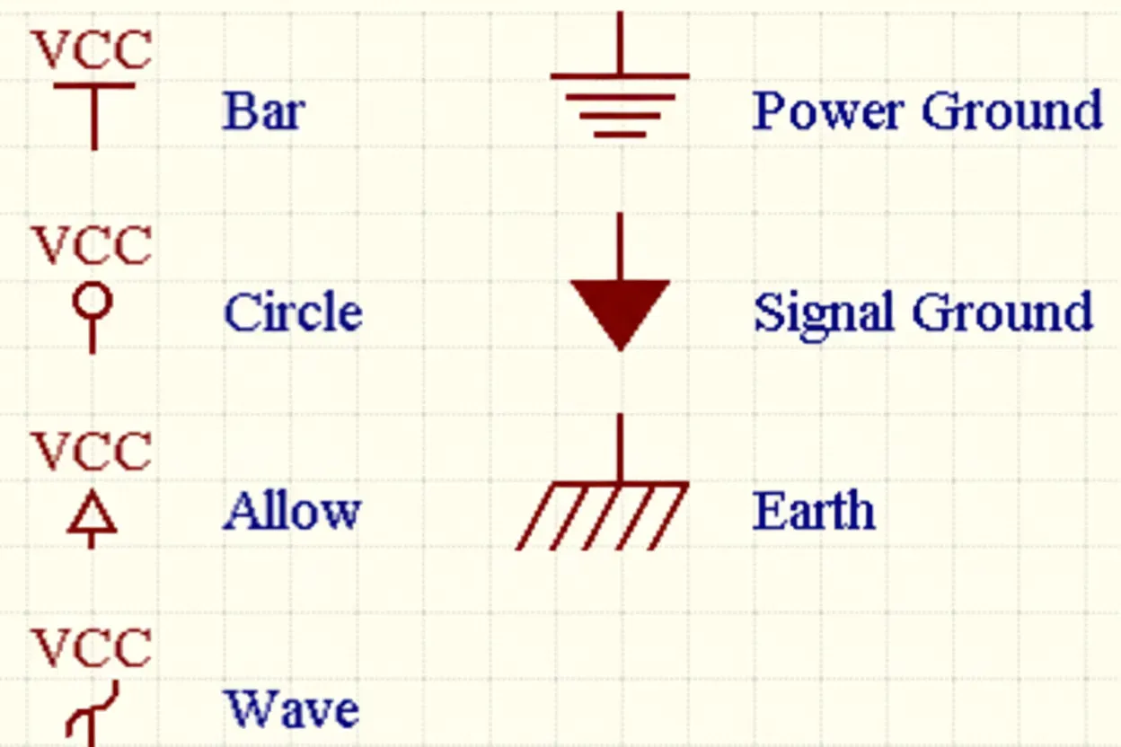
Perovskite and tandem cells exhibit greater sensitivity to environmental factors. This drives the need for low-noise analog front-end circuits on PCBs for accurate MPPT, voltage/current sensing, and stability monitoring. Controlled impedance routing and proper grounding are essential to maintain signal integrity near high-power switching sections.
Environmental Durability
Solar installations face extreme thermal cycling, humidity, and UV exposure. High-Tg materials, low-CTE laminates, and protective conformal coatings or potting are critical for long-term PCB reliability (25-30+ years).
Manufacturing Processes and Their Influence on System Design
Production methods for advanced cells - such as slot-die coating for perovskites and specialized annealing - highlight the importance of thermal uniformity. In field operation, this translates to PCBs that maintain stable performance across wide temperature ranges. Techniques like HDI layouts, back-drilling, and selective heavy copper plating help support compact, high-density designs in module-level power electronics (MLPE) and string inverters.
Testing, Stability, and Long-Term Reliability
Perovskite cells require rigorous stability testing under light, heat, humidity, and electrical stress. This data informs robust PCB design practices, including:
- Redundant sensing circuits
- Predictive maintenance features
- Enhanced solder joint reliability for vibration-prone installations
Emerging materials like graphene (with recent advances in epitaxial graphene semiconductors) may further improve thermal conductivity and switching speed in future power devices, allowing more compact and efficient PCB layouts.
Choosing the Right PCB Solution for Your Solar Application
Different solar cell technologies require tailored PCB strategies:
- Traditional crystalline silicon systems benefit from proven heavy copper and IMS solutions.
- Perovskite tandem deployments need advanced monitoring circuits and superior thermal management.
- Flexible or building-integrated PV favors rigid-flex PCB constructions.
Aivon provides comprehensive PCB manufacturing support for the entire solar value chain - from crystalline silicon to cutting-edge perovskite technologies. Our expertise in material selection, stack-up design, and high-reliability processing ensures your power electronics match the performance potential of modern solar cells.
For custom PCB solutions optimized for your specific solar cell type, inverter topology, or monitoring requirements, contact Aivon's engineering team to discuss technical specifications and DFM strategies.