Network security systems rely on sophisticated hardware to implement encryption, traffic inspection, threat detection, NAT traversal, monitoring, and policy enforcement. At the core of firewalls, IPS/IDS appliances, VPN gateways, SIEM collectors, and specialized security devices is high-performance PCB technology. These boards must handle high-speed data processing, cryptographic operations, low-latency interconnects, and continuous reliability under heavy enterprise loads.
At Aivon, we engineer and manufacture PCBs optimized for network security hardware. This article explores key security technologies, information attributes, key distribution methods, NAT traversal solutions, monitoring systems (including Kafka clusters), and common vulnerabilities - all through the lens of critical PCB design, material selection, fabrication processes, and reliability engineering.
Core Network Security Technologies and PCB Foundations
Modern network security combines multiple layers of protection:
- Firewalls, IPS/IDS, and UTM Systems: These perform deep packet inspection, anomaly detection, and real-time blocking. High-throughput requirements drive the need for multilayer PCBs (10-20+ layers) with controlled impedance routing, high-speed SerDes channels, and dedicated ASICs or NPUs.
- VPN and Encryption Gateways: Support secure tunnels and protocol handling, demanding strong cryptographic acceleration.
- Access Control and Authentication Systems: Integrate with key management infrastructure for policy enforcement.
These technologies place strict demands on PCB layout. Signal integrity becomes paramount for maintaining packet timing accuracy during inspection, while power integrity ensures stable voltage delivery to cryptographic engines during peak encryption loads.
Security Attributes and Their Impact on PCB Design
Effective network security rests on the CIA triad - Confidentiality, Integrity, and Availability - supplemented by authentication and non-repudiation.
- Confidentiality: Relies on robust encryption and secure key distribution. PCBs must support hardware security modules (HSMs) or trusted platform modules (TPMs) with isolated power domains, shielded layers for EMI protection, and low-noise clock distribution to prevent side-channel leakage.
- Integrity: Requires tamper-resistant hardware. This is achieved through precise lamination, high-quality etching for clean traces, and robust via structures that maintain signal fidelity across temperature variations.
- Availability: Systems must withstand attacks and maintain uptime. Thermal management solutions - including thick copper planes (2oz+), dense thermal via arrays, and high-Tg materials - prevent throttling during DDoS mitigation or sustained traffic surges.
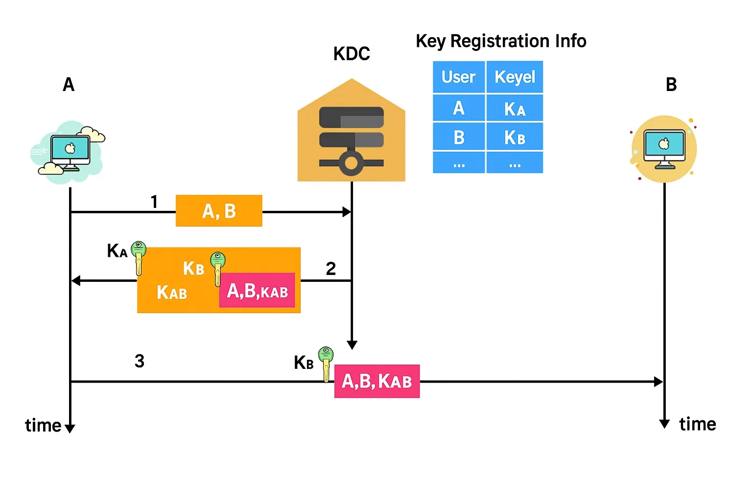
Key distribution mechanisms (symmetric, asymmetric, PKI, and Kerberos-style systems) further emphasize the need for precise timing circuits and low-jitter PCB designs to support secure session establishment without introducing vulnerabilities.
NAT Traversal Technologies and PCB Considerations
Network Address Translation (NAT) traversal is essential for enabling secure communication across private networks, particularly for VoIP, video conferencing, VPNs, and IoT devices. Common NAT traversal tools and principles include:
- STUN (Session Traversal Utilities for NAT): Helps endpoints discover public IP and port mappings.
- TURN (Traversal Using Relays around NAT): Provides relay services for symmetric NATs.
- ICE (Interactive Connectivity Establishment): Combines STUN and TURN for optimal path selection.
- UPnP and NAT-PMP: Automatic port mapping protocols.
Hardware implementations of NAT traversal (in firewalls, session border controllers, or NPS - Network Protection Systems) require PCBs capable of high concurrent session handling. This translates to dense interconnect designs, high-bandwidth memory interfaces for session tables, and excellent power delivery networks to maintain performance during traversal-heavy workloads. HDI PCBs with blind and buried vias helps achieve the port density and miniaturization needed in compact security appliances.

Network Monitoring Systems and Kafka Cluster Considerations
Comprehensive visibility demands specialized monitoring hardware and software. Types of network monitoring systems include:
- Passive monitoring (packet capture and analysis)
- Active monitoring (synthetic probes)
- Flow-based monitoring (NetFlow, sFlow)
- Application performance monitoring (APM)
Kafka cluster monitoring has become particularly important for high-volume security event streaming in SIEM and XDR platforms. Monitoring tools track throughput, consumer lag, partition health, and broker performance. The underlying hardware for these monitoring systems must process massive telemetry streams with minimal latency. PCBs for security monitoring appliances benefit from:

- Optimized stack-ups for high-speed Ethernet interfaces (25G/100G+)
- Low-loss laminates in RF-sensitive sections
- Advanced thermal dissipation to handle continuous logging and analytics loads
- Redundant power planes for high availability
Poor PCB design here can lead to dropped events, increased false negatives, or monitoring blind spots.
Common Network Security Vulnerabilities and PCB-Level Mitigation Strategies
Many vulnerabilities stem from misconfigurations, weak protocols, or implementation flaws, but hardware plays a decisive role in overall resilience:
- Protocol and Implementation Weaknesses: Buffer overflows or weak encryption can be exacerbated by unstable power delivery or signal degradation.
- Resource Exhaustion Attacks: DDoS and flooding attacks stress memory and processing. Robust PCBs with heavy copper, strategic decoupling capacitors, and thermal vias help maintain stability.
- Physical and Side-Channel Risks: Direct access or electromagnetic attacks are mitigated through proper grounding, shielding layers, and high-reliability surface finishes (ENIG or ENEPIG).
- Supply Chain and Manufacturing Risks: Inconsistent impedance or via quality can introduce subtle timing issues that attackers might exploit.
Comprehensive DFM analysis, impedance testing, thermal cycling, and burn-in validation during manufacturing significantly reduce these hardware-related failure modes.
Best Practices for PCB Manufacturing in Network Security Hardware
When designing and producing boards for security applications, focus on these areas:
- High-Speed Signal Integrity: Length matching, impedance control (+/- 10%), back-drilling, and minimized via stubs for multi-gigabit interfaces.
- Thermal and Power Management: Copper thickness optimization, thermal via farms under hot components, and multi-domain PDN design.
- Reliability Enhancements: High-Tg FR4 or advanced laminates, halogen-free materials, and HDI stack-ups for density and performance.
- EMI/EMC Compliance: Strategic layer arrangement and grounding practices essential for certification.
- Manufacturing Precision: Tight process control during etching, lamination, and drilling to ensure batch-to-batch consistency in high-stakes security deployments.
Conclusion
Network security success depends on the seamless integration of advanced technologies, monitoring capabilities, key management, NAT traversal, and vulnerability resilience. The printed circuit board serves as the fundamental platform that determines real-world performance, reliability, and security effectiveness.
Through expert PCB design and manufacturing - emphasizing signal integrity, thermal management, power distribution, and rigorous quality processes - organizations can deploy more capable and trustworthy security infrastructure. Aivon delivers specialized PCB solutions for network security device manufacturers, supporting everything from high-speed processing engines to reliable monitoring platforms.
For tailored PCB support in your security hardware projects, contact the Aivon engineering team to optimize stack-up, materials, and fabrication parameters for your specific performance and reliability targets.