Wearable devices continue to evolve from niche gadgets into essential tools for health monitoring, fitness tracking, and connected lifestyles. Yet sustained consumer adoption hinges not only on features and aesthetics but also on the underlying electronics—particularly the printed circuit boards (PCBs) that enable compact form factors, reliable sensor performance, efficient power management, and long-term durability in demanding real-world conditions.
For PCB manufacturers and design engineers, wearables present unique challenges in miniaturization, flexibility, thermal management, and environmental resilience. Addressing these at the board level directly influences user satisfaction, repeat purchases, and overall market growth.
Key Factors Influencing Wearable Device Adoption
Consumer research consistently highlights several priorities that shape purchase decisions for wearables. App ecosystem availability ranks highest, as users expect seamless integration with smartphones for data visualization, notifications, and third-party functionality. Devices lacking robust software support often fail to deliver meaningful daily value.
Demand for the latest technology drives upgrades, with buyers seeking smaller, faster, and more capable hardware. Appearance and fashion integration matter significantly because wearables are visible accessories; collaborations with style-focused brands help bridge the gap between technology and personal expression.
Price sensitivity remains critical—products must demonstrate clear value through consistent utility rather than novelty alone. Battery life stands out as a decisive usability factor. Devices requiring frequent charging quickly lead to abandonment, with many users discontinuing wear within months of purchase.
These adoption drivers translate directly into PCB-level requirements. Short, optimized traces and efficient power distribution networks reduce energy consumption. Advanced stack-ups and material selections support thinner, more flexible assemblies that maintain performance without adding bulk.
PCB Design Considerations for Wearable Success
Successful wearables demand PCBs that conform to the human body while withstanding continuous flexing, moisture exposure, and mechanical stress. Flexible and rigid-flex PCBs are preferred for their ability to follow natural contours in wristbands, smartwatches, shoes, and garments, minimizing stiffness and improving comfort.
Thermal management is essential. Processors, wireless modules, and sensors generate heat that can make devices uncomfortable against the skin. Copper thickness optimization, thermal vias, and strategic component placement help dissipate heat effectively without increasing overall thickness.
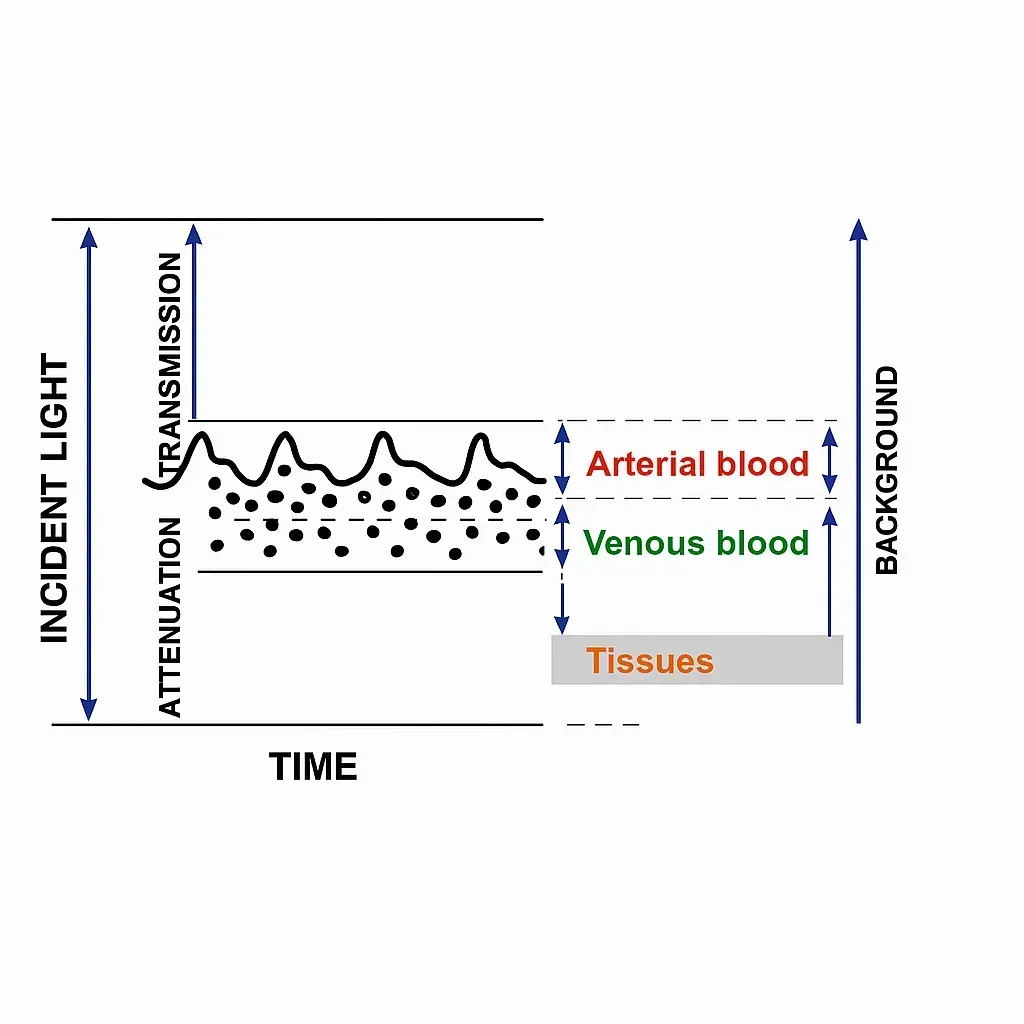
Signal integrity and electromagnetic compatibility (EMC) are paramount in compact layouts. High-density interconnect (HDI) techniques, controlled impedance routing, and proper grounding minimize noise in sensor data, ensuring accurate heart-rate, motion, and environmental readings even during vigorous activity.
Material choices further impact reliability. High-Tg laminates, specialized coatings, and moisture-resistant finishes protect against sweat, humidity, and repeated bending cycles. These decisions at the fabrication stage directly affect product lifespan and user retention.
Power delivery networks must support extended operation. Low-power design practices, efficient voltage regulation, and careful trace routing extend battery runtime, addressing one of the most common reasons for device abandonment.
Expanding Beyond Traditional Form Factors: PCB Implications for Emerging Wearables
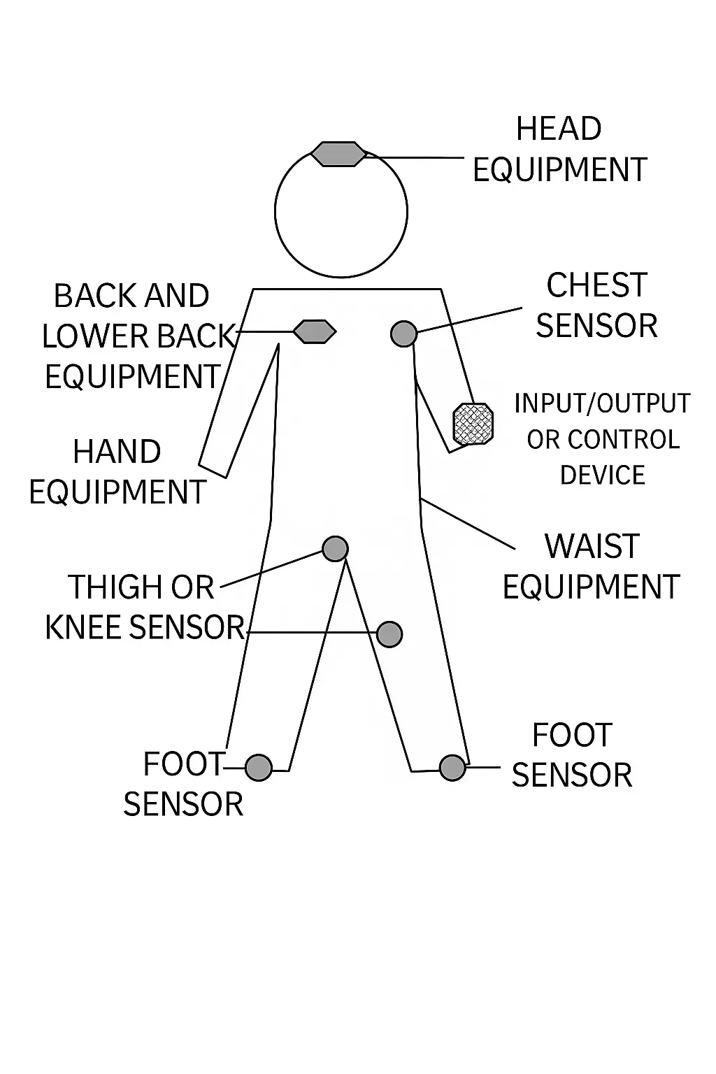
Innovation extends well beyond watches and fitness bands. Smart belts incorporate accelerometers, temperature sensors, and pressure elements to monitor activity, posture, and vital signs. These require compact, multilayer PCBs with integrated sensor interfaces and wireless connectivity modules.
Smart gloves combine displays, GPS, microprocessors, and even energy-harvesting elements such as solar cells. Flexible substrates enable integration across palm and finger areas while maintaining durability and providing protection.

Smart clothing and garments embed turn-signal lighting, cameras, and processing modules for safety and performance tracking. Here, stretchable or textile-integrated PCBs must balance conductivity with washability and comfort.

Each category introduces specific manufacturing considerations: precise via drilling for multilayer routing, selective soldering for mixed-technology assemblies, and rigorous testing for flex endurance and environmental sealing.
Smart Footwear and the Chinese Market: Opportunities for Specialized PCB Solutions
Footwear represents a massive opportunity in the wearable space. In China alone, the adult shoe market exceeds hundreds of billions in value, with billions of pairs produced annually. Smart running shoes integrate pressure sensors, accelerometers, GPS, and connectivity modules to deliver step counting, gait analysis, heart-rate monitoring, and location tracking.
Two primary categories dominate: step-counting models for fitness enthusiasts and location-tracking variants aimed at children or safety applications. Partnerships between traditional shoemakers, technology firms, and startups accelerate development, leveraging established supply chains alongside agile electronics innovation.
From a PCB perspective, smart shoes demand rugged, low-profile boards that fit within sole cavities while connecting to upper-mounted peripherals. Vibration resistance, waterproofing, and efficient power management under dynamic loading conditions are critical. HDI and flexible circuit techniques enable the dense sensor arrays and wireless functionality required without compromising shoe flexibility or comfort.

From Manufacturing to Long-Term Reliability and Future Outlook
Reliability begins at the fabrication stage. Controlled impedance, precise etching, and advanced lamination processes ensure consistent performance across temperature swings and mechanical stress. Failure analysis often traces back to issues such as delamination in flexible sections, insufficient thermal relief, or inadequate moisture barriers—problems that experienced PCB partners can mitigate through design-for-manufacturability (DFM) reviews.
As wearables proliferate across automotive, medical, industrial, and consumer sectors, demand grows for boards that support high-density components, low-power operation, and long-term stability. Manufacturers capable of delivering flexible, rigid-flex, and HDI solutions with tight tolerances position themselves as key enablers of the next generation of wearable technology.
Conclusion
Wearable device success ultimately depends on the quality and sophistication of the underlying PCBs. By prioritizing flexible and rigid-flex designs, advanced thermal and signal integrity management, robust material selection, and rigorous manufacturing processes, PCB engineers directly drive higher adoption rates, longer product lifespans, and greater user satisfaction. As the market expands into smart footwear, textiles, and beyond, collaboration between device developers and specialized PCB manufacturers will remain essential for turning innovative concepts into reliable, market-ready products that meet both consumer expectations and stringent engineering standards.