Wearable medical and consumer devices demand extreme miniaturization, ultra-low power consumption, and robust reliability while maintaining high signal integrity. At the heart of these requirements lies the printed circuit board, where material selection, stack-up design, via technology, and layout strategies directly determine device performance, battery life, and regulatory compliance. HDI PCB technology is particularly important for wearable devices because microvias, fine-line traces, and sequential build-up structures increase routing density without significantly increasing board thickness. These capabilities allow designers to integrate sensors, wireless modules, processors, displays, and power-management circuits into increasingly compact form factors.
How HDI Technology Helps Wearables Pack More Functionality Into Less Space
Modern wearables must fit within housings no larger than a coin cell while supporting multiple sensors, processors, and wireless modules. Wafer-level chip-scale packages (WLCSP) and ultra-thin four-layer PCBs with thicknesses around 0.5 mm enable this by allowing the package footprint to approach the die size itself. Designers cluster the microcontroller, accelerometer, LED indicator, and capacitive touch sensors near the board edge in a near-circular layout to maximize usable space and optimize user interaction zones.
For more demanding layouts, HDI PCB structures provide another level of miniaturization by replacing conventional through-hole connections with laser-drilled microvias and sequentially built interconnect layers. This allows routing to pass directly between adjacent layers, freeing additional surface area for fine-pitch components and reducing the overall PCB footprint. HDI PCB for wearable devices is therefore particularly useful when multiple functional blocks must coexist within a very limited mechanical envelope.
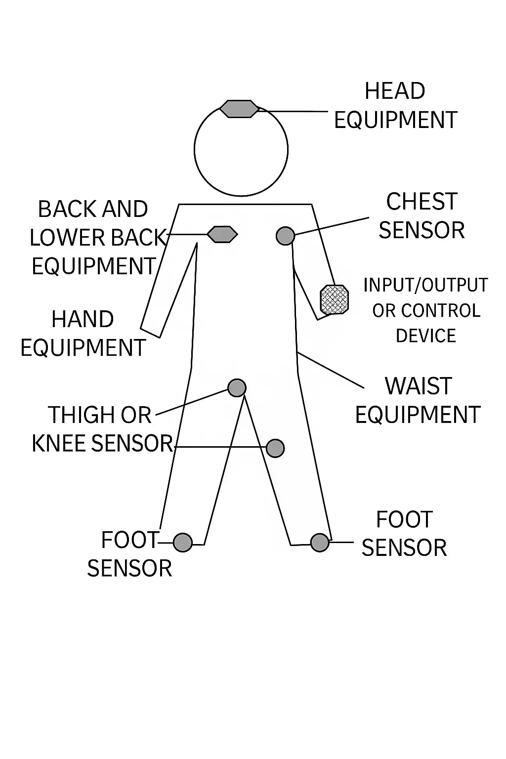
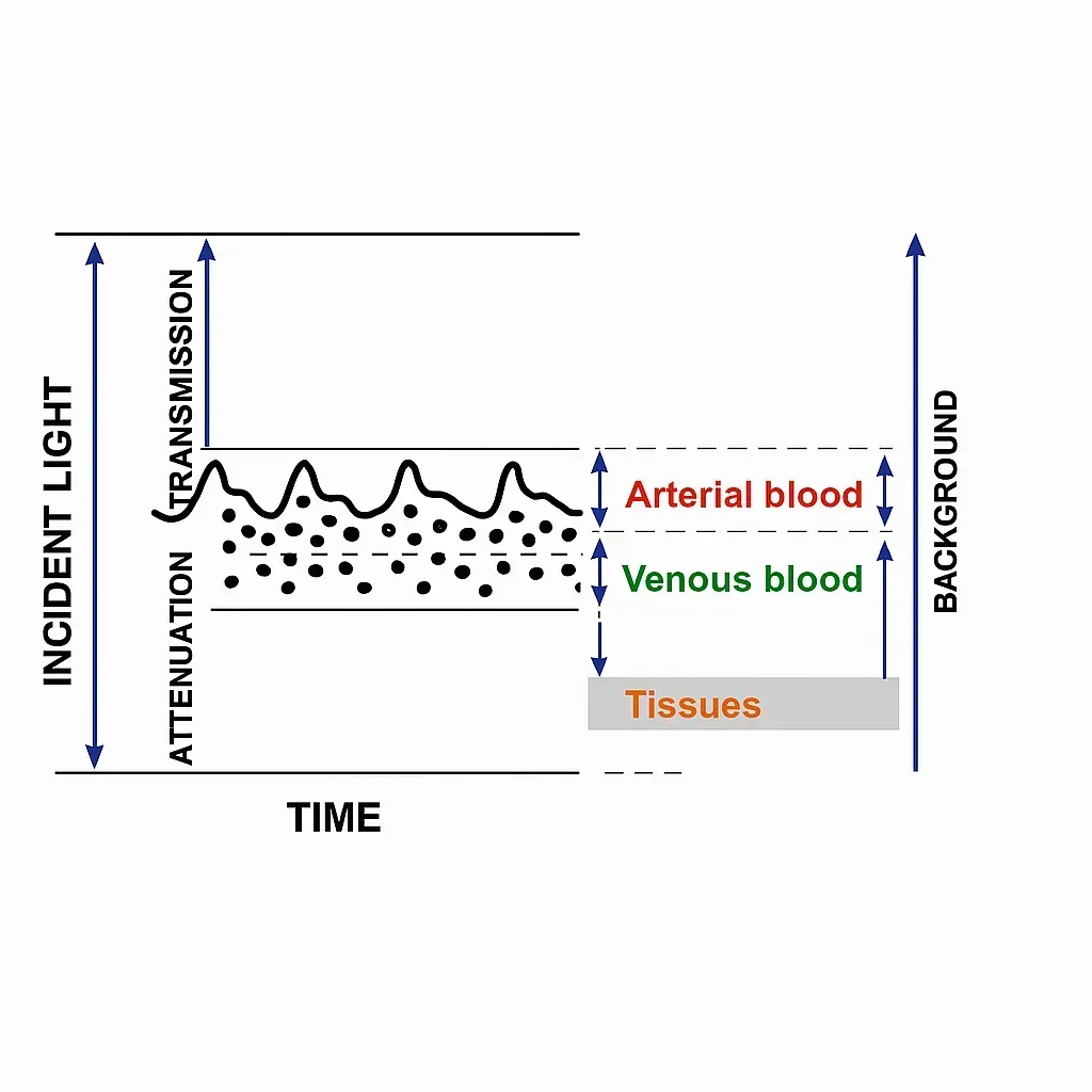
Component placement must balance mechanical stability with electrical performance. Symmetric positioning of inertial sensors minimizes offset errors, while short, shielded traces connect photodetectors or electrodes to analog front-ends. High-density interconnect (HDI) and microvia technology further increase routing density without increasing board thickness, supporting the fine-pitch footprints required for chip-scale MCUs.
Building Reliable Wireless and RF Performance Into Compact Wearable Boards
Wearable wireless networks rely on Bluetooth Low Energy, ZigBee, Wi-Fi, and NFC, each with distinct power and data-rate profiles. These radios operate in the 2.4 GHz ISM band and require controlled-impedance traces, proper antenna placement, and ground-plane stitching to maintain link reliability within the compact enclosure.
HDI PCB structures can help wearable designers route RF and digital signals through compact multilayer stack-ups while preserving controlled impedance and short signal paths. Microvias reduce the space consumed by conventional vias, allowing greater freedom in antenna keep-out zones and component placement. However, HDI density must be balanced with appropriate reference planes and via transitions to prevent unwanted coupling and signal discontinuities.
Hybrid network topologies—combining star and peer-to-peer configurations—allow sensors to communicate with a central master while supporting multi-hop data flow to smartphones or gateways. PCB-level power-management techniques, including adaptive transmission power control and isolated power domains, extend operating time on small lithium-polymer cells. Flexible polyimide substrates accommodate body-conforming form factors without compromising RF performance.

Designing the HDI PCB Around Sensors, Signal Integrity, and Real-Time Data
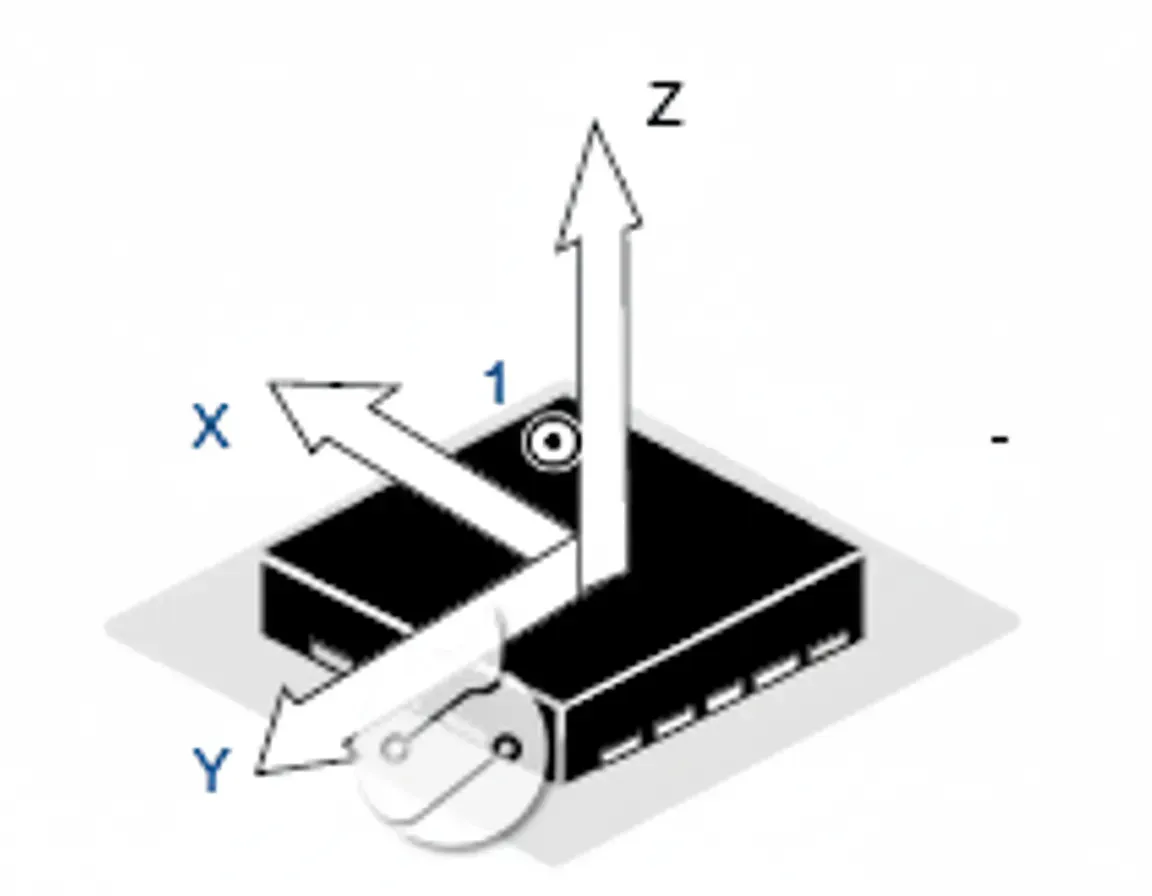
Accelerometers, optical heart-rate sensors, bioimpedance electrodes, and galvanic skin response detectors form the core sensing suite. Three-axis accelerometers measure inertial forces through suspended sensing elements whose voltage changes are digitized by onboard ADCs. PCB layout places these sensors near the board center with precise axis alignment to accurately capture gravity vectors (1 g) and dynamic motion patterns used for step counting, free-fall detection, and orientation recognition.
In HDI PCB wearables, the higher routing density provided by microvias and fine-line traces allows sensor interfaces to remain compact without forcing longer signal paths. This is particularly useful when several sensing channels must be positioned around a small central processor. Designers can use dedicated HDI layers for sensitive analog signals, power distribution, and high-speed digital connections while maintaining appropriate separation between noise-sensitive circuits.

Analog front-ends demand low-noise routing, guard rings, and dedicated ground planes to preserve microvolt-level signals amid motion artifacts. Multi-sensor fusion on the PCB—integrating accelerometer data with optical or impedance channels—enables real-time motion compensation and physiological parameter extraction while meeting strict power budgets.

Wireless Charging Receiver Integration on the PCB
Qi-compliant wireless charging receivers integrate synchronous rectification, battery management, and protection circuitry directly onto the board. Coil layouts must be optimized for electromagnetic coupling efficiency, with precise trace widths and spacing to minimize resistive losses. Foreign-object detection, over-current, over-voltage, and thermal protection features are implemented through careful component placement and thermal via arrays that dissipate heat away from skin-contact areas.
For compact wearable designs, HDI PCB technology can reduce the area required by supporting circuitry through microvias, fine-line routing, and compact component placement. Designers can separate power-management and control functions across dedicated layers while maintaining short interconnects between the charging receiver, battery-management IC, and protection circuits. Thermal considerations remain critical because higher routing density must not restrict heat dissipation paths.
High-integration receiver ICs with built-in MCUs and 12-bit ADCs reduce external component count, enabling thinner stack-ups and improved mechanical reliability under repeated flexing.

Display and Touch Panel PCB Interfaces
Wearable displays—Super AMOLED, P-OLED, and LCD panels—require tight integration with driver ICs and projected capacitive touch layers. On-cell or in-cell touch architectures reduce stack height while demanding precise impedance control on the PCB for touch sensing lines. Flexible or rigid-flex constructions support curved or circular display formats, with reinforced vias and conformal coatings ensuring durability during daily wear and disinfection cycles.
High pixel densities (up to 386 ppi) and haptic feedback drivers further increase routing complexity, making multilayer HDI PCBs for wearable devices particularly valuable for maintaining signal integrity without enlarging the overall device footprint. Microvias, fine-line traces, and via-in-pad structures allow display drivers and touch interfaces to connect through compact build-up layers, reducing routing congestion around high-pin-count components. This becomes increasingly important for circular displays and curved wearable form factors where available PCB area is highly constrained.
Human-Machine Interaction and PCB-Level Sensor Fusion
Seven primary interaction modalities—bone conduction audio, eye tracking, AR/MR overlays, voice, motion sensing, haptics, and emerging brainwave interfaces—each impose unique PCB requirements. Bone-conduction transducers and haptic actuators need robust mechanical mounting and low-noise drive circuits. Eye-tracking cameras and infrared emitters require precise optical alignment and high-speed digital routing. Haptic feedback systems demand fast-switching power delivery networks to deliver realistic tactile sensations.
As wearable devices combine more interaction functions within the same enclosure, HDI PCB structures provide the routing density needed to connect cameras, microphones, motion sensors, haptic drivers, and processing devices within limited board space. Shorter interconnects and compact via structures can also help control signal paths between these functional blocks.
Motion-sensing and voice interfaces rely on the same accelerometer and microphone signal-conditioning paths already optimized for health monitoring, enabling sensor fusion that reduces overall component count and power draw.
What It Takes to Manufacture Reliable HDI Boards for Everyday Wear
Producing reliable wearable PCBs requires sequential lamination for rigid-flex constructions, laser-drilled microvias, and automated optical inspection of fine-line features. For HDI PCB wearables, manufacturing consistency becomes particularly important because smaller vias, tighter line/space requirements, and multiple sequential build-up cycles leave less process margin than conventional PCB structures. Registration accuracy, microvia plating quality, via filling, and dielectric thickness must therefore be tightly controlled throughout production.
Biocompatible surface finishes, high-Tg laminates, and moisture-resistant conformal coatings ensure long-term performance in skin-contact environments. Accelerated life testing that simulates flex cycles, temperature swings, and sweat exposure validates design margins before volume production.
By treating the PCB as the central engineering platform that simultaneously solves miniaturization, thermal, signal-integrity, power, and mechanical challenges, manufacturers can deliver wearable devices that combine clinical-grade accuracy with consumer-friendly comfort and longevity.
Where Wearable PCB Technology Is Heading: Stretchable, Embedded, and AI-Ready Designs
Emerging wearable applications are pushing printed circuit board technology toward greater flexibility, integration density, and intelligence. HDI and UHDI technologies are becoming increasingly important as wearable products demand smaller footprints while adding sensors, wireless functions, displays, and local processing. Stretchable and hybrid rigid-flex-stretchable constructions are transitioning from research to production, combining rigid islands for active components with ultra-thin elastomeric interconnect layers. These designs allow the PCB to conform to skin movement without stressing solder joints or sensor contacts, enabling multi-week continuous monitoring patches that integrate ECG, PPG, and bioimpedance sensors on a single board.
Ultra-high-density interconnect (UHDI) PCBs with line/space below 20 µm and embedded-component technology are becoming standard for extreme miniaturization. By burying microcontrollers, power-management ICs, and memory die inside the stack-up, designers achieve board thicknesses under 0.4 mm while supporting higher sensor counts and display driver integration. This directly benefits smart rings, earbuds, and curved-display wearables that require both compact footprints and robust mechanical reliability.
On-board edge AI is driving new PCB-level power-domain isolation, high-speed memory routing, and advanced thermal via arrays. Neural processing units integrated directly into the board enable real-time motion compensation, arrhythmia detection, and voice recognition without cloud dependency, while maintaining safe skin-contact temperatures during continuous operation.
Advanced substrate materials are entering volume manufacturing. Liquid-crystal polymer (LCP) and graphene-enhanced copper foils deliver superior high-frequency performance for 5G/6G and UWB wireless systems, while bio-based and partially biodegradable laminates address emerging sustainability requirements without sacrificing electrical or mechanical stability. For displays and touch interfaces, in-cell architectures combined with rigid-flex constructions reduce stack height while maintaining precise impedance control.
Wireless power transfer and multi-modal energy harvesting are now designed at the PCB level. Optimized coil layouts, rectenna integration, and piezoelectric or thermoelectric harvesters embedded in the stack-up enable months-long operation with minimal user intervention. Hardware-rooted security features—such as secure elements and physical unclonable functions—are implemented directly in the board layout to protect physiological data from acquisition through transmission.
Conclusion
Advanced PCB design forms the foundation of every high-performance wearable device. Miniaturization, signal integrity, thermal management, wireless performance, display integration, and human-machine interaction all converge on precise material selection, stack-up optimization, via technology, and layout strategies. As the industry advances toward stretchable electronics, embedded AI, sustainable materials, and hardware-level security, manufacturers who master these PCB-level innovations will deliver the next generation of reliable, comfortable, and intelligent wearable healthcare and consumer technology.
FAQ
Q1: What are the benefits of HDI PCB for wearable devices?
A1: HDI PCB for wearable devices enables higher circuit density within smaller board footprints. Microvias, fine-line routing, and advanced stack-ups allow designers to integrate more sensors, processors, wireless modules, and power-management components without increasing device size. This approach supports thinner wearables, improved signal integrity, shorter interconnects, and greater design flexibility for smartwatches, health monitors, earbuds, and other compact electronics.
Q2: How does HDI PCB technology improve wearable device miniaturization?
A2: HDI PCB technology increases routing density through microvias, fine-line traces, and sequential build-up structures. These features allow components to be placed closer together while reducing the space required for conventional through-hole vias. For wearable devices, this makes it possible to integrate multiple sensors, wireless circuits, displays, and processors into compact board areas while maintaining electrical performance and mechanical reliability.
Q3: What should you look for in an HDI PCB manufacturer for smartphones and wearable devices?
A3: An HDI PCB manufacturer for smartphones and wearable devices should demonstrate strong capabilities in microvia drilling, sequential lamination, fine-line fabrication, and multilayer registration. Manufacturers should also provide reliable quality control, material selection, impedance control, and testing processes. Experience with rigid-flex or flexible constructions can be particularly valuable when producing compact devices that require mechanical flexibility and consistent electrical performance.
Q4: Why are microvias important for HDI PCB wearables?
A4: Microvias are essential for HDI PCB wearables because they connect densely routed layers without requiring the larger space occupied by conventional vias. Laser-drilled microvias support finer-pitch components and shorter signal paths, helping designers fit sensors, wireless modules, processors, and power circuits into small wearable boards. Proper microvia design and plating also contribute to reliable performance during repeated bending, thermal cycling, and everyday use.