










PCB Specifications
| Parameter | Value | Parameter | Value |
|---|---|---|---|
| PCB Type | Rigid-Flex PCB | Quantity | 10 pcs |
| Layers | 7 Layers | Board Type | Single PCB |
| Dimensions | 256.23 x 67.05 mm | Copper Weight | 1OZ |
| Thickness | 1.6 mm | Min Track / Spacing | 6/6mil↑ |
| Surface Finish | ENIG (Immersion Gold) | Min Hole Size | 0.3mm↑ |
| Solder Mask | Black | Silkscreen | White |
Manufacturing Timeline
Logistics Information
Key Manufacturing Processes
Manufacturing Summary
This rigid-flex construction measured 256.23 × 67.05 mm and combined a multi-layer flexible section with rigid FR-4 areas to form an overall 7-layer stack. Produced as 10 single pieces, the order used ENIG surface finish (1.0 µin Au over 120–200 µin Ni), black coverlay on the flex region, black solder mask on the rigid sections, and white silkscreen. Finished thickness targets were 1.6 ± 0.16 mm for the rigid portion and 0.5 ± 0.05 mm for the flex section. Copper weights were adjusted to ½ oz inner / 1 oz outer on the flex and 1 oz throughout the rigid areas. The 27-day schedule required IPC Class 3 acceptance, full flying-probe testing, thermal-stress reports, and micro-section analysis.
DFM review resolved multiple material, via, and process constraints. The original stackup and material call-outs were revised to available grades (Shengyi SF202 for the flex core and S1000-2 for the rigid portions) while preserving the target thicknesses. PI stiffener locations and sizes were not clearly defined in the source data and were omitted. Via treatment was changed from mixed openings to full tenting; certain 0.6 mm vias were accepted with possible hole-mouth discoloration and residual ink, while 0.2 mm vias carried a residual risk of incomplete development and ink intrusion. Extra pads appearing on one solder-mask layer were clarified, independent adhesion pads were added on inner layers, and production numbering was omitted because no location or content was specified. Black ink could not meet the required chemical resistance, so green PSR-4000 GEC50A was substituted after confirmation. J1 was not supplied and was left unpopulated; J2 had already been assembled.
Confirmed stackup, material substitutions, via-mask decisions, and assembly scope were implemented prior to production. The rigid-flex panels achieved consistent ENIG plating, controlled thickness, and reliable coverlay adhesion within the planned timeline. Full electrical, thermal-stress, and micro-section reports accompanied the shipment, confirming the boards met the IPC Class 3 and dimensional requirements.
Explore More PCB Manufacturing Resources
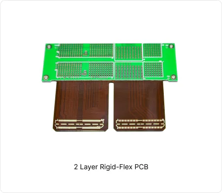
2 Layer Rigid-Flex PCB Manufacturing Insights
2 layer rigid-flex PCBs combine a double-sided flexible polyimide circuit with selective rigid sections in a single board. Uses polyimide flex core with FR-4 or polyimide stiffeners. Supports coverlay on flexible areas and solder mask on rigid zones.
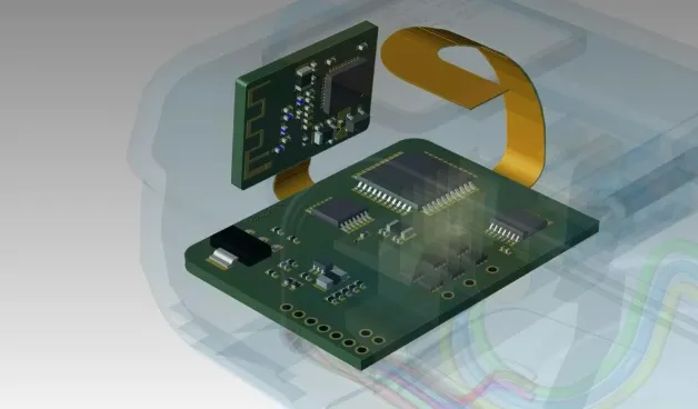
The Ultimate Guide to Rigid-Flex PCB Design: Mastering Reliability, Complexity, and Cost
Master the complexities of Rigid-Flex PCB Design with this 2,500-word guide. Explore stack-up symmetry, bend radius calculations, via optimization, and cost-effective manufacturing strategies.
Real Production Records
| Order ID | PCB Type | Layers | Dimensions | Solder Mask | Surface Finish | Quantity | Action |
|---|---|---|---|---|---|---|---|


