










 00:50
00:50
Component Placement
Component placement is a critical aspect of printed circuit board (PCB) design that directly influences the functionality, reliability, and manufacturability of electronic assemblies. When engineers and designers search for guidance on component placement, they often seek strategies to optimize board layout for better signal integrity, thermal management, and ease of assembly. This tag encompasses a range of topics, from fundamental principles to advanced techniques, helping users address common challenges such as minimizing electromagnetic interference, reducing trace lengths for high-speed signals, and ensuring adequate spacing for heat dissipation. In practice, effective component placement begins with understanding the schematic and prioritizing components based on their roles. For instance, placing sensitive analog components away from noisy digital sections can prevent crosstalk, while grouping power regulators near high-current loads improves efficiency and reduces voltage drops. Best practices also include considering mechanical constraints, such as connector positions for user interfaces or mounting holes for enclosures, to streamline the transition from design to production. By adhering to these guidelines, designers can avoid costly revisions and enhance overall board performance, whether working on consumer electronics, automotive systems, or industrial controls. For those delving deeper into specific scenarios, articles under this tag offer detailed case studies and step-by-step tutorials. You might find insights on automating placement with CAD software or troubleshooting issues in multilayer boards, providing the tools needed to refine your designs. As PCB complexity grows with emerging technologies like IoT and 5G, mastering component placement remains essential for achieving robust, high-performing circuits.
Video Guide

Technical Articles
Why a Small Footprint-Origin Shift Moves Every Pick-and-Place Coordinate
Boost PCB Design Efficiency with Interactive Cross-Probing and Modular Placement
Fast Component Alignment in Altium Designer for Cleaner PCB Layouts
How to Continuously Place the Same Symbol in a KiCad Schematic
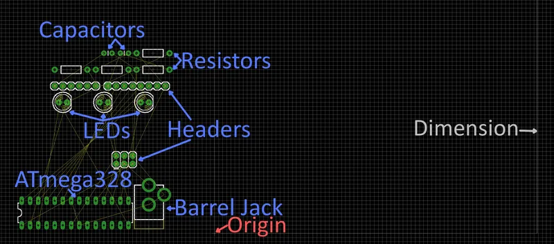
Stuck on PCB Placement? First Arrange These Four Types of Positions
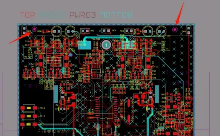
PCB Fiducials: Small Marks That Impact Production
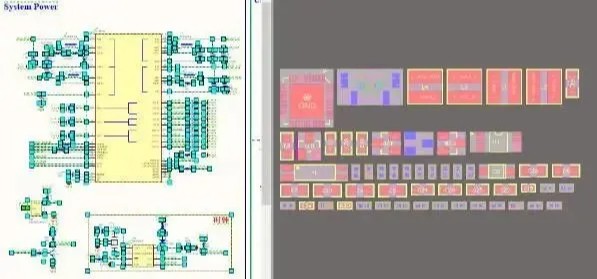
Interactive and Modular PCB Layouts to Double Design Efficiency
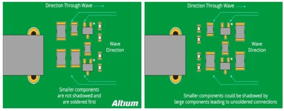
Six Practical PCB Design Techniques That Avoid Common Manufacturing Problems
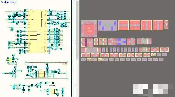
Interactive and Modular Placement to Improve PCB Design Efficiency
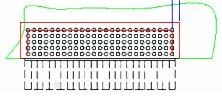
Why Moving a Component Only 1 mm from a Press-Fit Connector Still Causes Assembly Interference
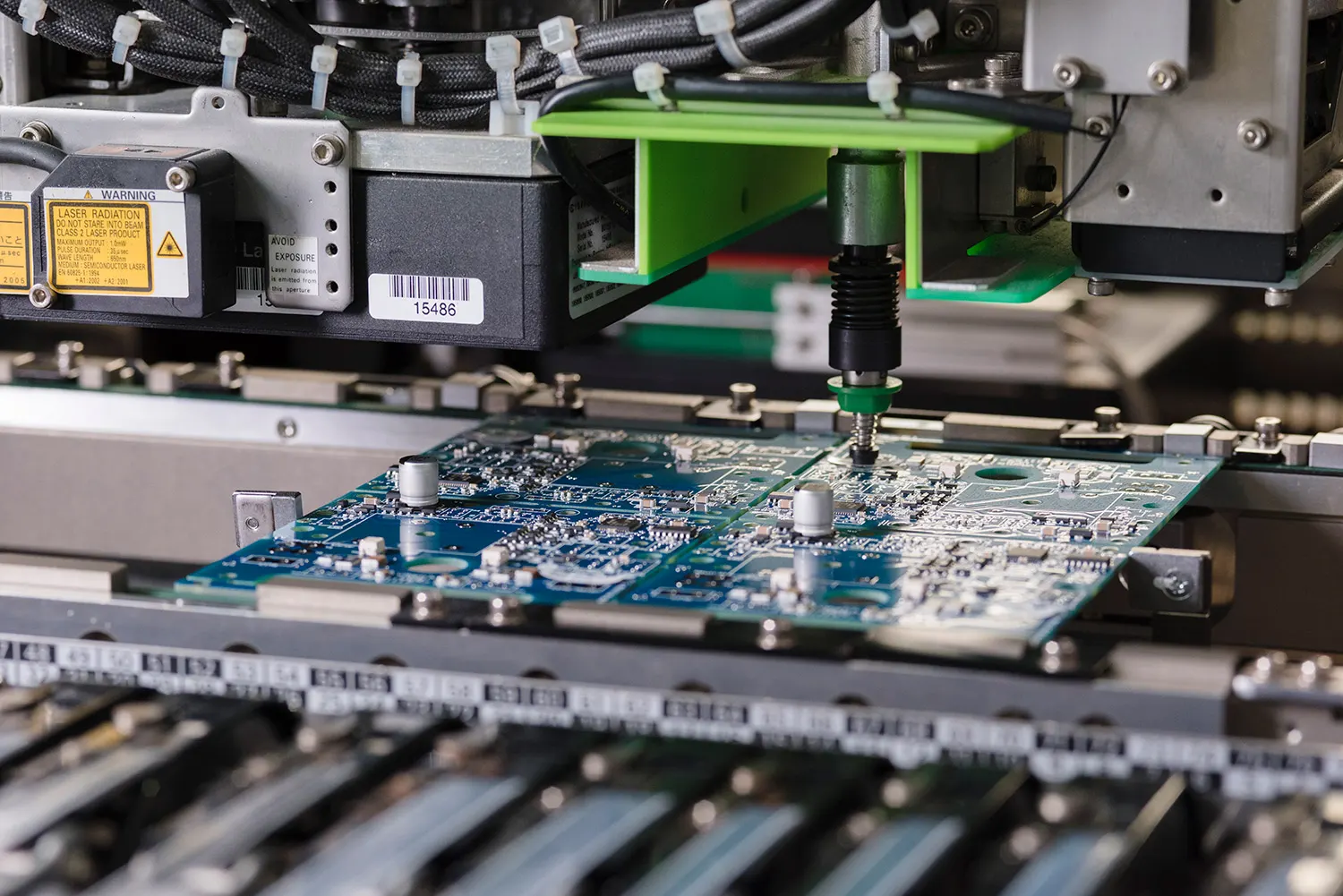
Design for Assembly Checklist: 10 Steps to Streamline Your PCB Assembly Process
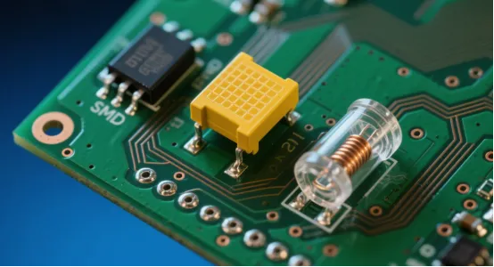
SMD Fuses: Compact Circuit Protection for High Density PCBs
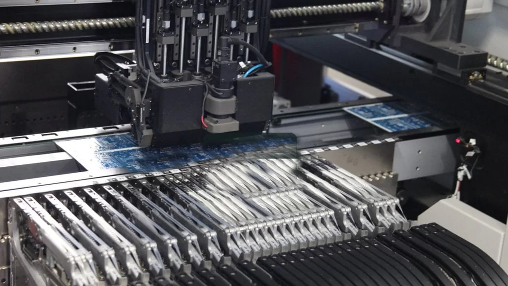
The Ultimate Guide to Design for Assembly (DFA) in Electronics Manufacturing
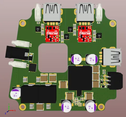
Mastering Miniaturization: PCB Design Tips for Compact Fitness Devices
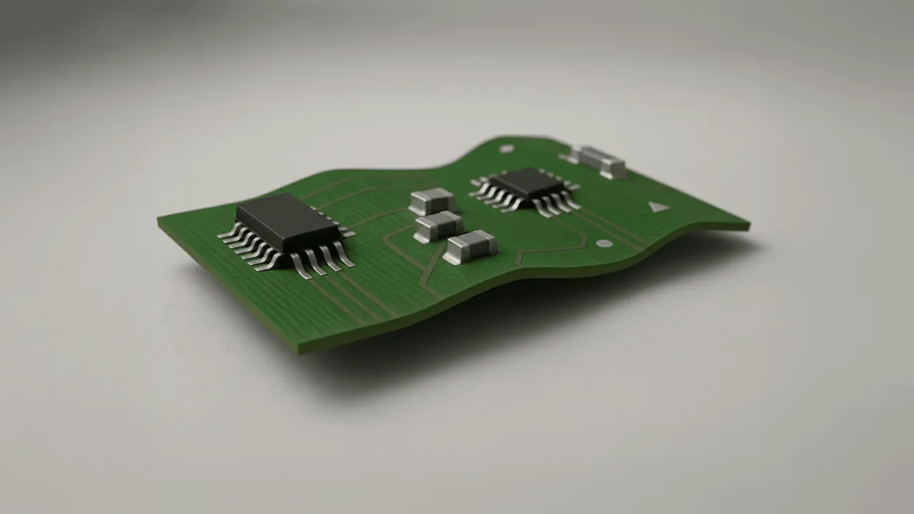
Troubleshooting Common Issues in PTFE PCB Assembly
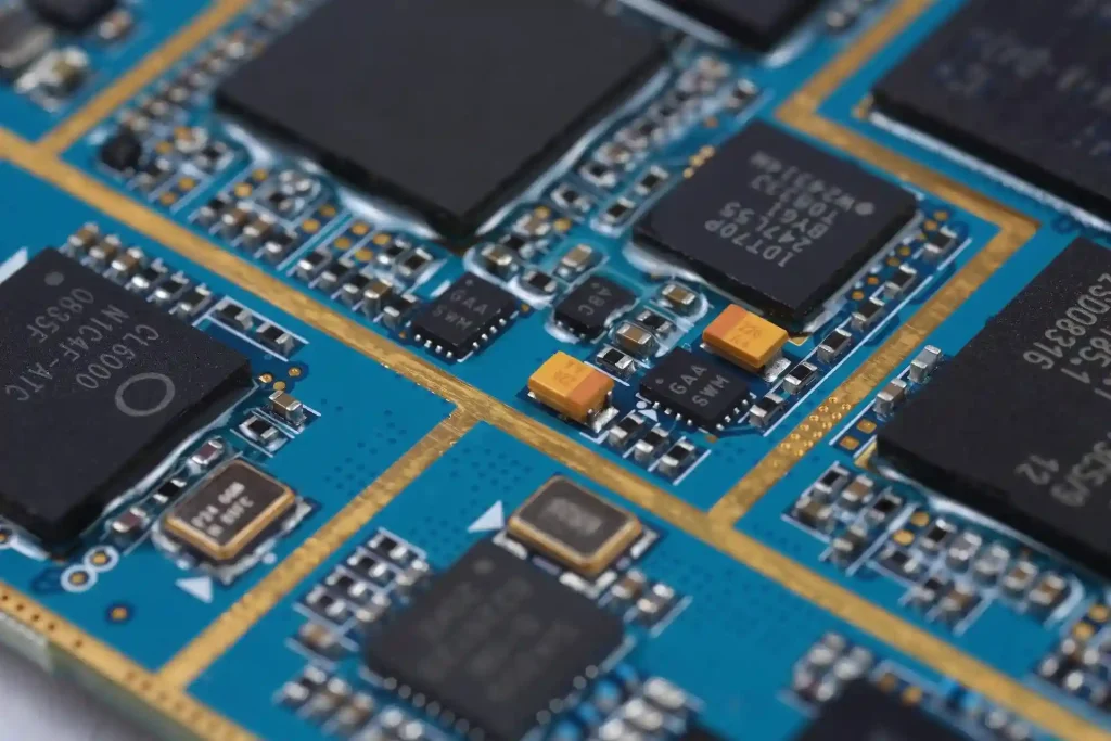
Shielding Component Placement: Optimizing Performance Through Strategic Design
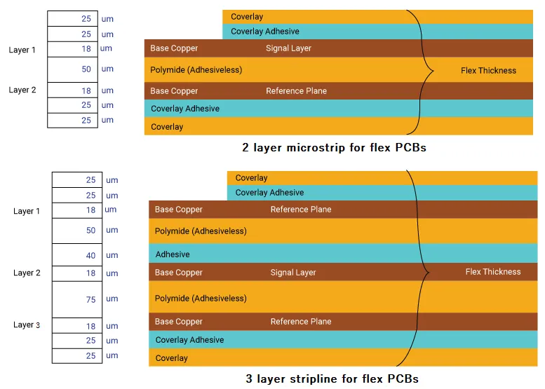
Beyond the Board: Mastering Flexible PCB Assembly for Reliability
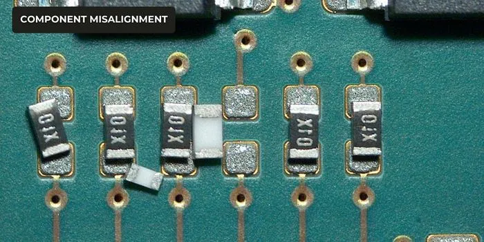
Troubleshooting Component Misalignment in PCB Manufacturing: A Practical Guide
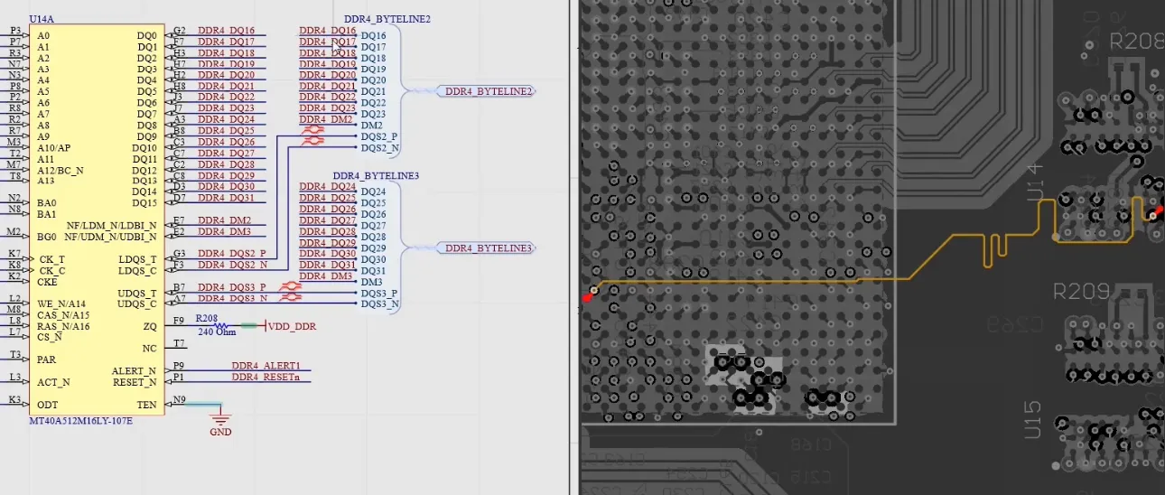
PCB Design Review for Beginners: A Step by Step Guide


