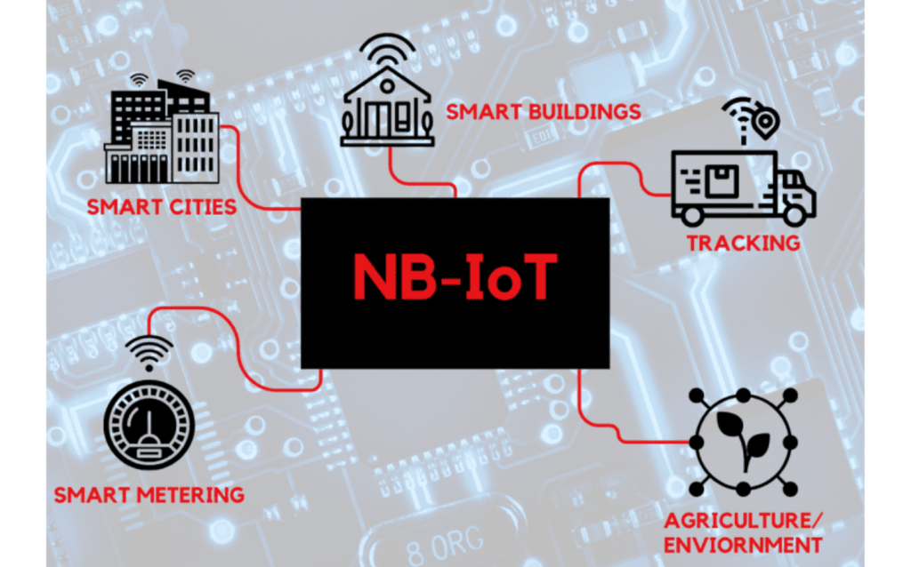
NB-IoT has emerged as a key narrowband cellular technology for low-power, wide-area IoT deployments. Its combination of extended coverage, ultra-low power consumption, and support for massive device density makes it particularly suitable for battery-operated sensors and actuators in smart homes, metering, industrial monitoring, and connected infrastructure. From a PCB manufacturing standpoint, successful NB-IoT implementations depend on optimized board-level design for RF performance, power integrity, thermal management, and long-term reliability under real-world environmental conditions.
Classification of IoT Communication Technologies and PCB Implications
IoT wireless technologies are broadly divided into short-range and wide-area categories. Short-range options such as Zigbee, Wi-Fi, Bluetooth, and Z-Wave dominate indoor smart-home applications but suffer from limited range and interference in larger or multi-story dwellings. Wide-area LPWAN technologies address these gaps; NB-IoT operates in licensed spectrum and delivers the coverage, capacity, and security advantages of cellular networks while maintaining extremely low power and cost profiles.
On the PCB, the choice of wireless technology directly influences layout strategy. Short-range modules require careful antenna placement and isolation to minimize self-interference, while NB-IoT designs demand precise RF trace routing, controlled impedance, and robust grounding to achieve the deep indoor penetration and extended coverage that define the technology. Multilayer PCBs with dedicated RF layers and proper via stitching help maintain signal integrity across the narrowband spectrum.
Evolution of 3GPP MTC Technologies and Hardware Requirements
Before NB-IoT, 3GPP advanced machine-type communication through successive LTE-MTC categories and GSM evolutions aimed at lower cost, lower power, and enhanced coverage. NB-IoT consolidated competing proposals into a unified standard optimized for low-data-rate, battery-powered endpoints.
These standardization efforts translate into concrete PCB requirements. NB-IoT modules must support deep sleep modes and power-saving features that place strict demands on power delivery networks. Designers use low-leakage decoupling capacitors, optimized power planes, and careful partitioning between analog/RF and digital domains to prevent noise coupling that could degrade receiver sensitivity or increase current draw. High-Tg laminates and appropriate copper weights further ensure stable performance across temperature variations typical in home and industrial environments.
Standardization Process and Its Impact on PCB Module Design
The 3GPP process that unified NB-CIoT and NB-LTE proposals into a single NB-IoT specification emphasized coexistence with existing GSM/UMTS/LTE networks, reduced terminal complexity, and minimal hardware impact on base stations. The resulting standard supports module costs competitive with or below legacy 2G solutions.
For PCB manufacturers and designers, this standardization simplifies component selection and supply-chain planning. Pre-certified NB-IoT modules with standardized pinouts and interfaces reduce custom RF engineering effort. However, integration still requires attention to antenna matching, EMI shielding, and mechanical constraints. Rigid-flex or multilayer stack-ups with controlled dielectric properties help maintain consistent RF performance across high-volume production runs.
Smart Home Challenges and PCB-Centric Solutions
Deploying NB-IoT in smart homes addresses four primary industry pain points, each with direct PCB implications:
- Ease of use and installation — Complex pairing and setup are mitigated by reliable wireless links. PCBs must deliver stable RF performance and low-power operation so devices remain responsive without frequent battery changes.
- Network capacity and coverage — Dead zones in bathrooms, balconies, or large homes require strong link budgets. PCB-level antenna design, ground plane optimization, and strategic component placement extend effective range and reduce retransmissions that waste energy.
- Security — Hardware-level protections, including secure element integration and robust power/ground isolation, complement protocol-level security. Proper PCB layout prevents side-channel leakage and supports tamper-resistant module mounting.
- Fragmented standards and interoperability — Standardized NB-IoT interfaces on the PCB enable multi-vendor ecosystems. Consistent module footprints, connector options, and test-point layouts simplify assembly and validation across different smart appliance platforms.

NB-IoT Solutions for Smart Homes: PCB Integration Considerations
Solutions such as open application frameworks built on NB-IoT provide device SDKs, client libraries, and gateways that abstract protocol complexity. At the hardware level, these frameworks rely on PCBs that combine the NB-IoT modem with sensors, MCUs, and power management ICs.
Critical PCB design elements include:
- Low-power analog front-ends for sensor interfaces
- Efficient switching regulators with minimal EMI
- Compact layouts supporting MEMS sensors and secure elements
- Thermal relief features even in low-power designs to handle occasional high-current transmission bursts
Manufacturing considerations encompass tight impedance control for RF sections, precise drilling for via-in-pad where space is limited, and panelization strategies that preserve antenna performance across batches.
Key PCB Engineering Challenges for NB-IoT Devices
Successful NB-IoT products must overcome recurring board-level constraints:
- Power integrity and ultra-low leakage — Multiple voltage domains and extended sleep currents require careful decoupling and layout to avoid leakage paths.
- RF performance and EMI/EMC — Narrowband operation benefits from clean spectrum; star grounding, guard traces, and shielding cans protect receiver sensitivity.
- Thermal and environmental reliability — Even low-power devices experience temperature cycling in homes; high-Tg materials and robust via structures enhance longevity.
- Miniaturization and cost optimization — HDI or multilayer constructions accommodate dense integration while supporting high-volume, cost-sensitive production.
Manufacturing Best Practices and Cross-Industry Applications
Partnering with experienced PCB manufacturers ensures optimized stack-ups, material selection, and assembly processes tailored to NB-IoT requirements. These practices extend across automotive telematics, industrial sensors, smart metering, and medical wearables—any application demanding reliable, long-life wireless connectivity on a constrained power budget.
By addressing signal integrity, power efficiency, and manufacturability from the earliest design stages, engineers can deliver NB-IoT devices that meet both the technical targets of the 3GPP standard and the practical demands of real-world IoT deployments.
Conclusion
NB-IoT technology delivers the coverage, power efficiency, and scalability required for next-generation IoT and smart home systems, yet its performance ultimately depends on the underlying PCB. Optimized RF layout, power integrity, EMI control, and material selection directly determine link budget, battery life, and long-term reliability. Manufacturers that apply rigorous PCB engineering practices—from controlled-impedance stack-ups to precise via and grounding strategies—enable devices that maintain consistent operation across diverse environments while supporting cost-effective, high-volume production. As NB-IoT deployments continue to expand, close collaboration between system designers and PCB specialists remains essential to achieving both technical targets and commercial success.