High-performance audio systems in smartphones, wireless earbuds, portable speakers, and professional sound reinforcement rely on precise PCB engineering. From moving-coil loudspeakers and power amplifiers to digital signal processing and low-phase-noise clocking, every element of the audio chain depends on optimized PCB layout, material selection, thermal management, signal integrity, and manufacturing processes.
Aivon delivers the multilayer, HDI, and rigid-flex PCB solutions required to meet the demanding electrical, thermal, and mechanical constraints of modern audio electronics.
Moving-Coil Loudspeaker Integration and PCB Crossover Networks
Moving-coil loudspeakers operate on electromagnetic induction principles, where current through the voice coil interacts with the permanent magnet's field to produce mechanical motion. The voice coil, former, and magnet assembly must interface with the amplifier and crossover circuitry, which are almost always implemented on a PCB.
PCB designers place passive or active crossover networks directly on the board to divide the audio spectrum between woofers, midrange drivers, and tweeters. Low-inductance trace routing, proper component placement, and controlled impedance are essential to maintain phase coherence and prevent insertion loss. High-current paths to the voice coil require thicker copper (2 oz or more) and wide traces to minimize resistance and heating.
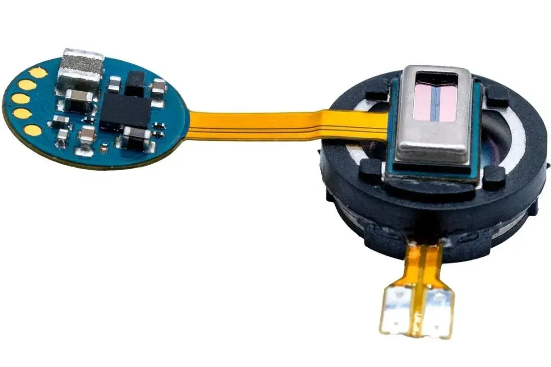
In compact portable devices, flexible or rigid-flex PCBs allow the crossover and protection circuitry to conform around the driver assembly, reducing parasitic inductance and improving mechanical reliability under vibration.
Power Amplifiers and Thermal Management on PCB
Class-AB and Class-D audio power amplifiers such as the LM4766 demand robust PCB power delivery networks. The device's high output current and associated heat generation require low-impedance power and ground planes, multiple thermal vias under the package, and strategic heatsink attachment points.
Designers select high-Tg laminates and increased copper thickness in power sections to improve heat spreading. Proper via stitching connects top-layer copper pours to inner power planes, lowering thermal resistance and preventing localized hot spots that degrade audio fidelity or trigger thermal protection.
For mobile audio solutions, compact PCB layouts must also incorporate EMI filtering and decoupling capacitors close to the amplifier pins to suppress switching noise and maintain low distortion across the audio band.
Digital Audio Clocking and Low-Phase-Noise PCB Layout
Digital audio performance hinges on low-jitter, low-phase-noise clock sources. SCTF-grade oscillators and PLLs require careful PCB implementation: dedicated analog power domains, star grounding, and short, shielded clock traces to minimize coupling from digital switching noise.
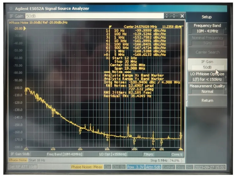
Multilayer stack-ups with dedicated ground planes beneath clock circuits provide return paths that reduce radiated emissions and preserve signal integrity. Controlled-impedance routing and guard traces further isolate sensitive clock lines from adjacent digital or power signals.
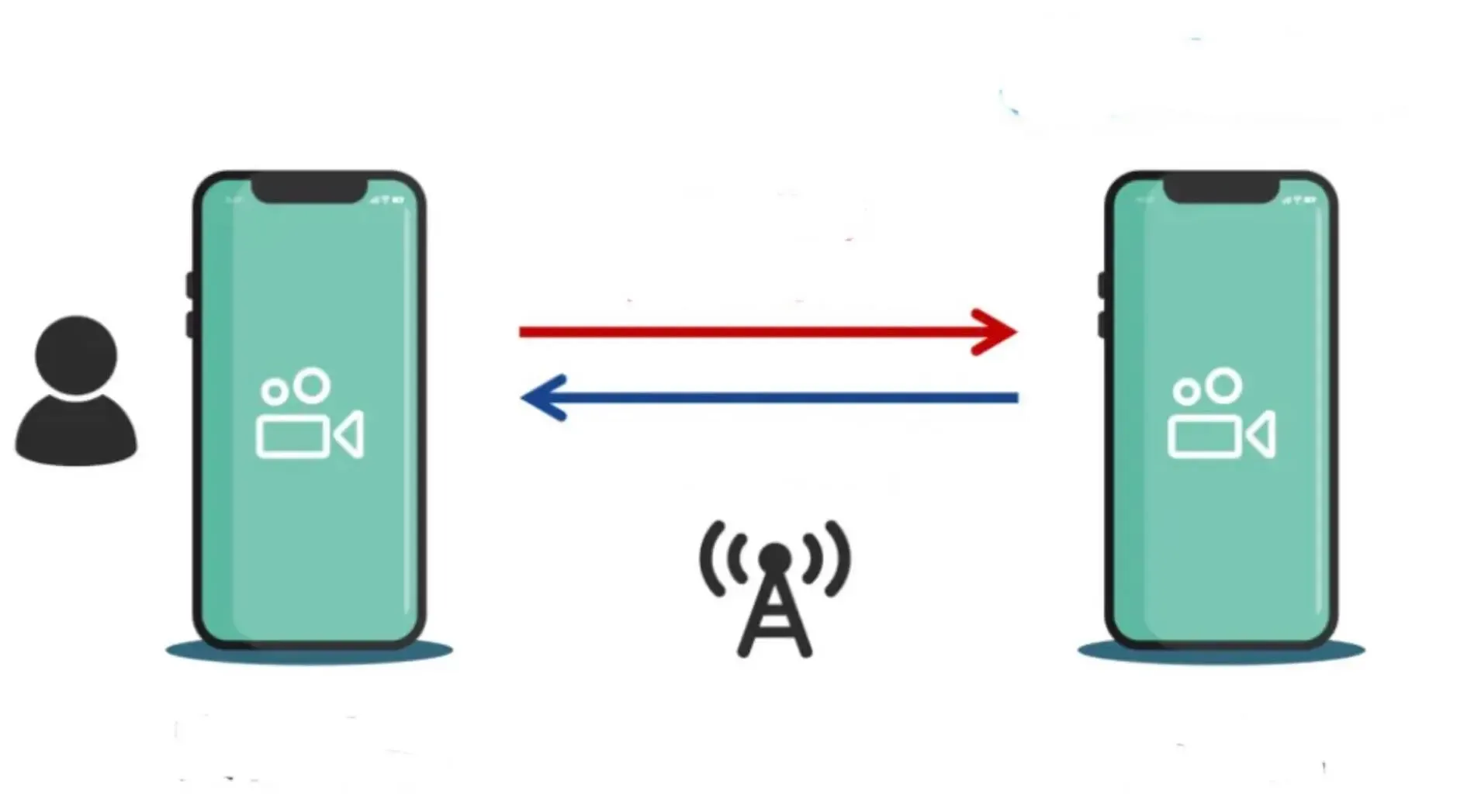
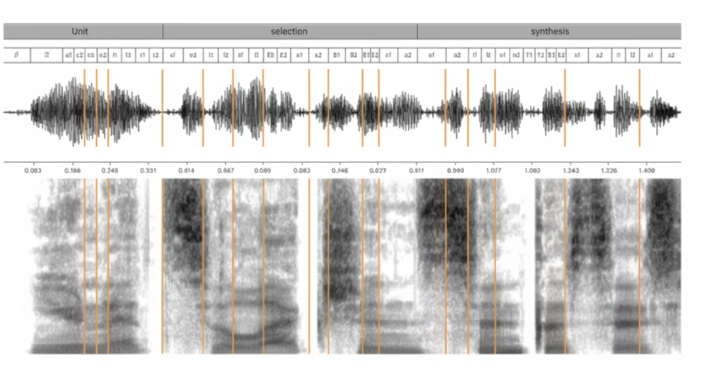
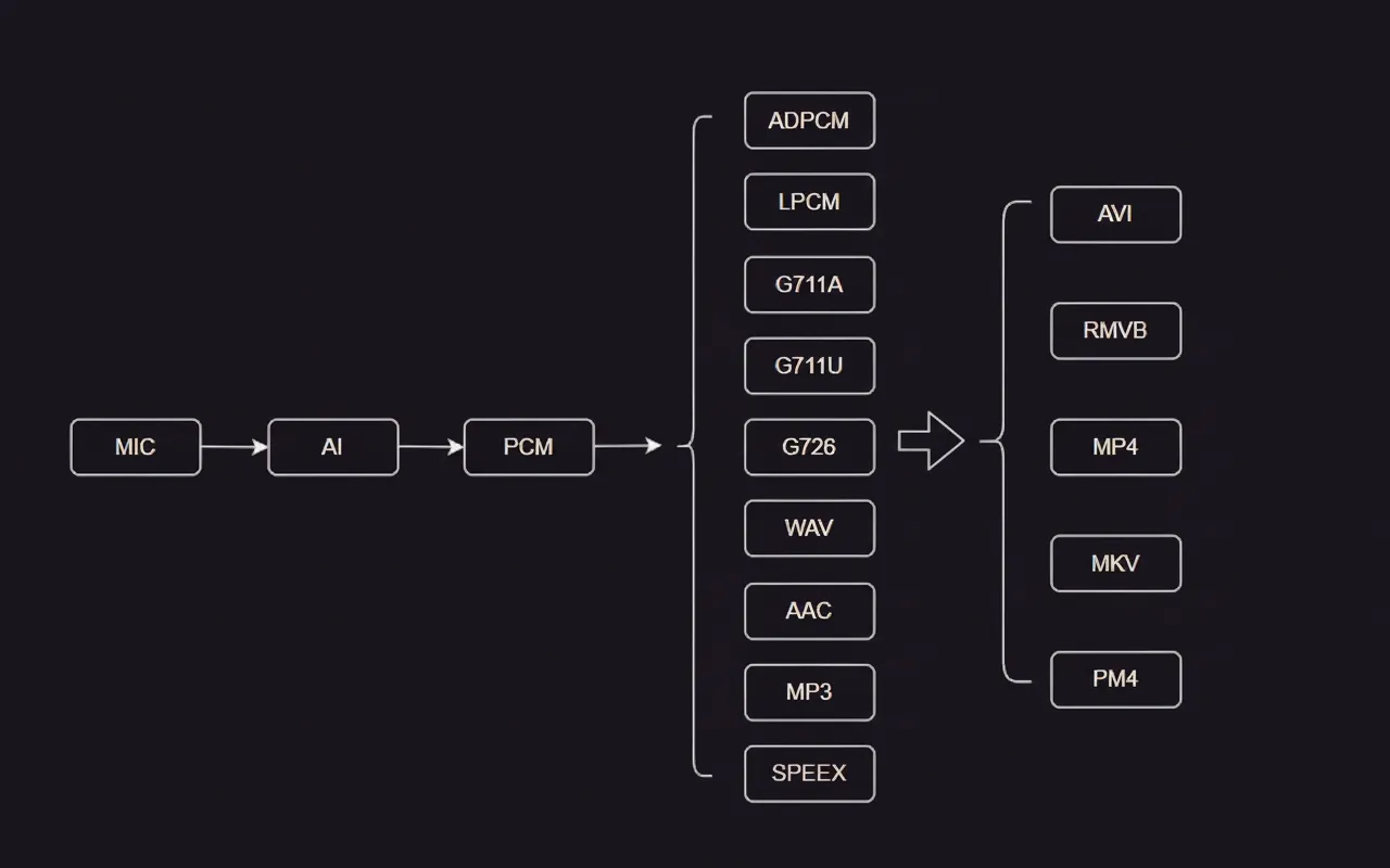
In embedded audio processing workflows, the PCB must support high-speed serial interfaces (I²S, TDM) while maintaining tight timing margins, often necessitating HDI features or back-drilled vias to control stub length.
High-Resolution Audio Requirements and PCB Signal Integrity
High-resolution audio (24-bit/96 kHz and beyond) extends bandwidth and dynamic range demands compared with standard 16-bit/44.1 kHz formats. PCB layout must accommodate wider frequency response, lower noise floors, and reduced crosstalk.
Designers employ differential signaling, symmetric trace lengths, and low-dielectric-loss materials (e.g., Rogers or specialized FR4 variants) in analog sections. Power supply rejection and grounding strategies become critical to prevent digital noise from modulating the analog output.
In NXP smart audio platforms and similar SoC-based designs, the PCB integrates DSP cores, DACs, and amplifiers on a single board, requiring meticulous partitioning of analog, digital, and power domains with proper moating and stitching vias.
Testing, Measurement, and Manufacturing Considerations
Audio measurement platforms such as the AP525 rely on ultra-low-noise PCB designs for accurate characterization of THD+N, frequency response, and intermodulation distortion. Reference-grade PCBs use star grounding, shielded compartments, and precision voltage references to achieve the required measurement floor.
During volume manufacturing, tight control of trace width, dielectric thickness, and via quality ensures consistent audio performance across production batches. Surface finishes such as ENIG or OSP are chosen to maintain low contact resistance on connector and test points.
For large-scale installations such as school auditoriums, the system PCB must support long cable runs, robust power distribution, and fault-tolerant grounding schemes while complying with EMI/EMC regulations.
Reliability, EMI/EMC, and Cross-Industry Applications
Audio PCBs must suppress electromagnetic interference from switching power supplies, wireless modules, and digital processors. Techniques include ground planes, shielding cans, ferrite beads on power lines, and careful component orientation.
Consumer, automotive, and professional audio applications share common PCB challenges: vibration resistance, wide temperature operation, and long-term reliability under continuous use. High-reliability laminates, filled vias, and conformal coating options help meet these requirements.
Future Trends in Audio PCB Technology
Wide-bandgap semiconductors and GaN-based Class-D amplifiers will drive higher switching frequencies, enabling smaller magnetics and demanding PCB materials with lower loss tangents at RF. AI-assisted layout tools will optimize trace routing and via placement for minimal distortion and EMI.
Flexible and stretchable PCBs will enable conformal audio modules in wearables and foldable devices. Sustainability initiatives are accelerating adoption of halogen-free and recyclable substrates. HDI and substrate-like PCB technologies will continue to shrink footprints while supporting higher channel counts and integrated DSP.
Conclusion
Successful audio system performance ultimately depends on PCB-level engineering decisions. By addressing electromagnetic coupling in loudspeakers, thermal paths in power amplifiers, signal integrity in digital clocks and high-resolution converters, and robust manufacturing processes, designers achieve the clarity, efficiency, and reliability demanded by today's market.
Aivon's advanced PCB fabrication capabilities—multilayer stack-ups, precise impedance control, thermal via optimization, and HDI features—provide the foundation for next-generation audio electronics across consumer, mobile, and professional applications.