Wearable devices such as smart bands, wristbands, and emerging automotive key fobs must deliver accurate health monitoring, seamless wireless connectivity, and robust data protection within extremely constrained form factors. From a PCB manufacturing perspective, these requirements translate directly into multilayer stack-up optimization, high-density interconnect (HDI) techniques, flexible and rigid-flex substrates, secure hardware integration, and rigorous signal integrity and EMI control.
Aivon supports wearable OEMs with advanced PCB fabrication capabilities that address the unique electrical, thermal, mechanical, and security challenges of next-generation personal electronics.
Privacy and Hardware Security at the PCB Level
Data privacy risks in wearables stem primarily from wireless transmission, on-device storage, and potential physical tampering. PCB-level countermeasures include dedicated secure elements or trusted platform modules (TPMs) mounted on the board, hardware-accelerated encryption engines within the main SoC, and tamper-evident routing that detects enclosure breach.
Designers implement secure boot and encrypted firmware storage through isolated power domains and controlled-impedance traces that prevent side-channel attacks. Ground planes and shielding layers further reduce radiated emissions that could leak sensitive biometric information. In high-security applications such as automotive key fobs, automotive-grade laminates with enhanced temperature and vibration resistance ensure long-term reliability of these security features.

Sensor Integration and Analog Front-End PCB Design
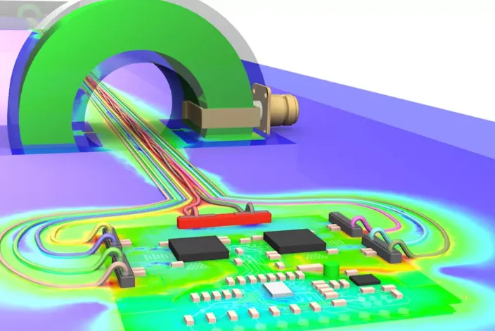
Accurate health data tracking relies on precise analog front-end circuitry for PPG, ECG, accelerometer, and temperature sensors. PCB layout must minimize noise coupling between sensitive analog traces and digital switching signals through careful partitioning, star grounding, and dedicated analog power planes.
High-resolution ADCs demand low-dielectric-loss materials and matched trace lengths to preserve signal integrity. Flexible PCB sections allow sensors to conform to the wrist or body while maintaining stable electrical connections to the rigid main board. Via-in-pad and microvia technologies reduce parasitic inductance in high-speed sensor interfaces, improving measurement accuracy and reducing motion artifacts.
Power Management, Thermal Dissipation, and Battery Life Optimization
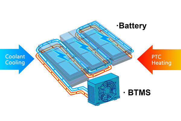
Persistent challenges in wearables—limited battery capacity, heat generation, and continuous operation—are directly addressed through PCB power delivery network (PDN) design. Low on-resistance MOSFETs, efficient DC-DC converters, and optimized copper pours minimize I²R losses. Strategic placement of thermal vias under power ICs and the use of high-Tg or metal-core substrates improve heat spreading in ultra-thin enclosures.
For devices using nRF51822 or similar Bluetooth Low Energy SoCs, PCB designers balance RF performance with power efficiency by selecting appropriate antenna matching networks, ground plane cutouts, and decoupling strategies. Rigid-flex constructions allow the battery and charging circuitry to occupy separate mechanical zones while maintaining reliable high-current paths.
Miniaturization, Flexible Substrates, and HDI Technologies
Size constraints drive adoption of HDI PCBs with laser-drilled microvias, fine-line traces, and sequential lamination. These techniques enable higher component density and shorter interconnect lengths, critical for integrating multiple sensors, wireless modules, and secure elements on boards smaller than a coin.
Flexible and rigid-flex PCBs provide mechanical compliance for wrist-worn devices and allow the antenna and display sections to fold or curve around the enclosure. Material selection—polyimide or liquid crystal polymer (LCP) substrates—ensures low moisture absorption and stable dielectric properties across temperature and humidity ranges encountered in daily wear.
RF Integration, Antenna Design, and EMI/EMC Compliance
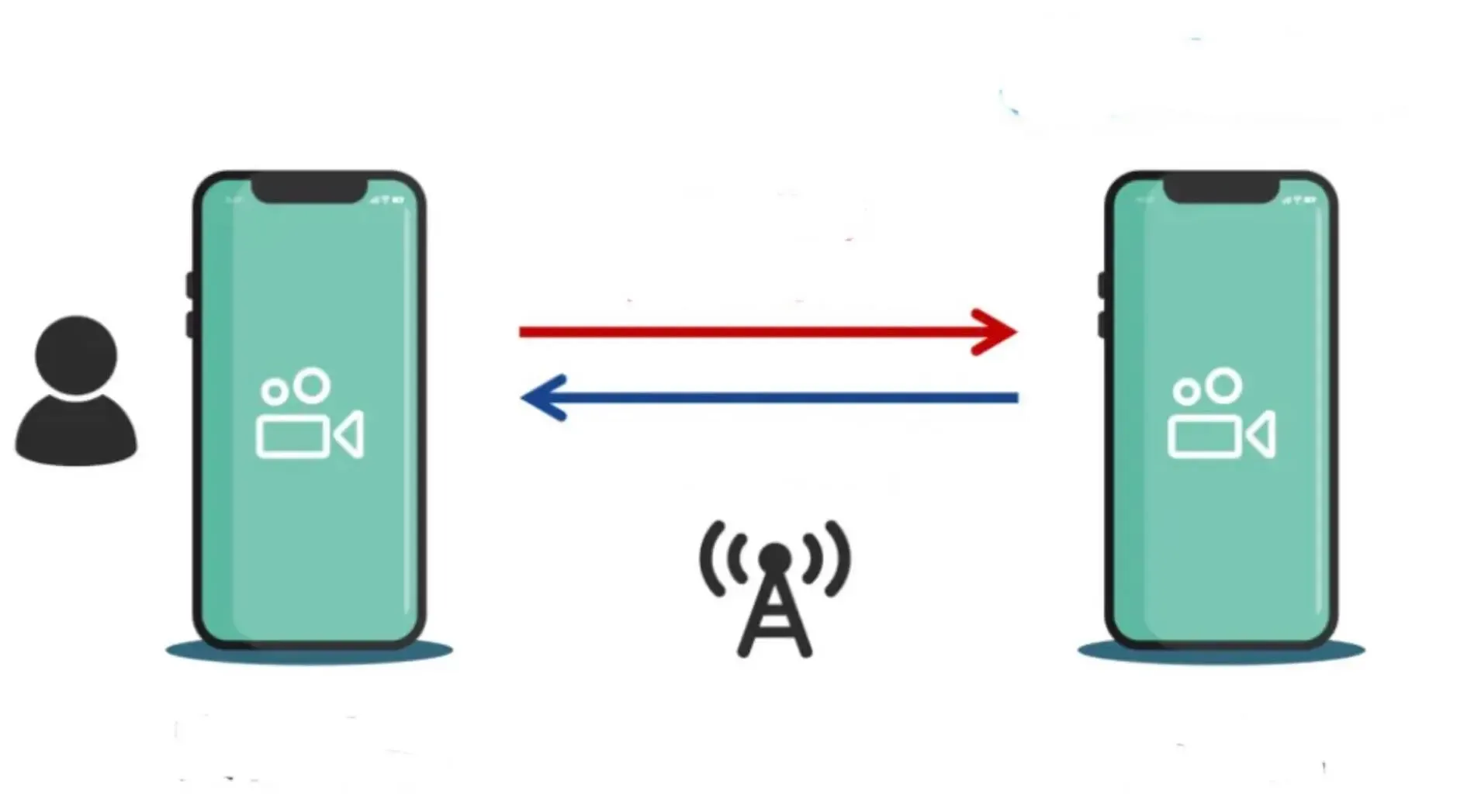
Wireless connectivity in wearables requires careful PCB antenna design and layout. Bluetooth, NFC, and emerging UWB modules demand controlled impedance, proper ground plane referencing, and isolation from digital noise sources. Shielding cans, guard traces, and ferrite beads help meet stringent EMI/EMC regulations while preserving receiver sensitivity.
In automotive wearable key applications, PCB-level RF performance must remain stable across wide temperature swings and vibration profiles, often requiring automotive-qualified laminates and enhanced via plating.
Reliability, Manufacturing, and Cross-Industry Applications
Wearable PCBs must withstand sweat, temperature cycling, mechanical flexing, and long-term storage. Conformal coating options, filled vias, and high-reliability surface finishes (ENIG, ENEPIG) improve corrosion resistance and contact reliability. Manufacturing tolerances on trace width, dielectric thickness, and via quality directly impact device-to-device consistency in biometric accuracy and wireless range.
Beyond consumer fitness bands, the same PCB engineering principles apply to medical-grade wearables, industrial safety monitors, and automotive access systems, where failure can have serious consequences.
Future Trends in Wearable PCB Technology
AI-optimized layout tools will further reduce noise and power consumption in sensor and RF sections. Stretchable and printed electronics will enable fully conformal sensor arrays. Higher integration of secure elements and neuromorphic processors will demand advanced substrate-like PCB (SLP) and embedded-component technologies. Sustainability requirements are accelerating the use of halogen-free and recyclable materials without compromising electrical performance.
Conclusion
Secure, accurate, and long-lasting wearable devices ultimately depend on PCB-level engineering excellence. By focusing on hardware security features, precise analog and RF layout, efficient power and thermal management, and advanced miniaturization techniques, manufacturers can overcome the persistent challenges of size, battery life, privacy, and reliability.
Aivon's expertise in HDI, rigid-flex, and high-reliability PCB fabrication provides the technical foundation for the next generation of personal electronics that users can trust with their health data and daily convenience.