Wireless power transfer (WPT) has become essential for modern portable devices, enabling cord-free charging of smartphones, wearables, TWS earbuds, and power banks. From a PCB manufacturing perspective, successful WPT implementation demands precise layout of coupling structures, optimized power-conversion circuitry, robust thermal management, and careful material selection to balance efficiency, size, reliability, and cost.
Aivon supports these requirements through advanced PCB fabrication capabilities tailored to consumer electronics applications.
Electromagnetic Coupling Technologies and PCB Integration
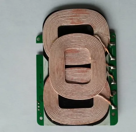
Electromagnetic coupling remains the dominant approach for WPT due to its superior efficiency compared with acoustic or optical alternatives. Traditional inductive power transfer (IPT) relies on magnetic fields generated by coils, but it faces challenges including sensitivity to misalignment, limited penetration through metal enclosures, and higher electromagnetic interference (EMI).
Resonant magnetic coupling improves distance and alignment tolerance by tuning transmitter and receiver circuits to the same frequency. Capacitive power transfer (CPT) offers an alternative using electric-field coupling across paired conductive plates. CPT systems can transfer power through thin metal barriers when modeled as series capacitors and generally produce lower EMI because the electric field is more confined.
For PCB designers, IPT typically requires dedicated transmitter and receiver coils—either as discrete components or embedded traces in multilayer or flexible PCBs. CPT implementations use closely spaced conductive plates or patterns on the PCB surface or within the stack-up. Both approaches benefit from precise control of trace geometry, dielectric properties, and layer stack-up to maintain resonance and minimize parasitic losses.
Advances in printed electronics and MEMS integration further enable compact CPT interfaces suitable for low-power portable devices such as wireless chargers and earbud cases.
Power Conversion Efficiency and PCB Power Delivery Networks
Early WPT architectures regulated output using resistive methods, incurring significant conduction and switching losses. Modern designs replace these with switching power supplies and optimized rectifier bridges, achieving system efficiencies approaching or exceeding 90% in well-engineered implementations.
On the PCB, efficiency gains come from low on-resistance MOSFETs in synchronous rectification, minimized trace resistance in power paths, and proper decoupling to reduce switching noise. The receiver-side circuitry must handle AC-to-DC conversion followed by DC regulation while maintaining tight control over bias networks.
For TWS earbud charging cases and portable power banks, voltage-following or low-dropout charging topologies dramatically improve end-to-end efficiency. Solutions that dynamically adjust the case output voltage to stay only slightly above the earbud battery voltage (e.g., ~50–75 mV difference in constant-current phase) can push linear charger efficiency near 98%, compared with ~74% in conventional 5 V fixed-output designs. This approach reduces heat generation and extends case runtime by 20–30% without requiring additional software intervention or large inductors.
PCB layout must support these topologies through careful placement of sense resistors, current-monitoring paths, and low-impedance power planes. Multilayer boards with dedicated power and ground layers help maintain signal integrity and thermal performance.
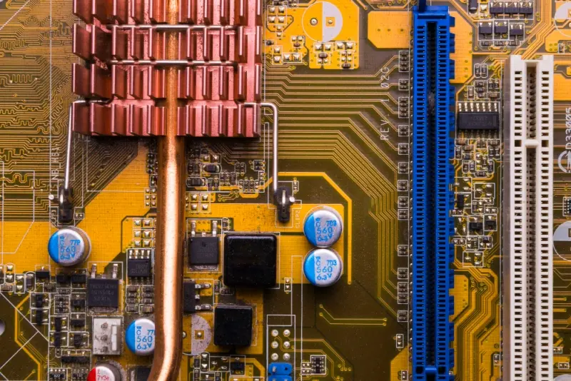
Thermal Management and Material Selection for WPT PCBs
Heat dissipation is a critical constraint in compact portable devices. Elevated temperatures accelerate lithium-ion battery degradation and can reduce component reliability. PCB design directly influences thermal performance through copper thickness, via placement for heat spreading, and choice of substrate materials.
High-Tg FR4 or specialized laminates with improved thermal conductivity are often selected for power-dense sections. Thicker copper layers (2 oz or more) in power paths lower I²R losses and improve heat spreading. In wireless charging modules, strategic via stitching under coils or power ICs creates effective thermal vias to inner layers or heatsink planes.
For power banks and charging cases, the PCB must also accommodate battery protection circuits, boost converters, and wireless transmitter coils while preventing localized hot spots that could affect nearby batteries or user comfort.
Battery Management and Charging Circuit Design Considerations
Modern lithium-ion batteries in portable devices require sophisticated management to maximize cycle life and safety. PCB-level implementations include protection against overcharge, over-discharge, overcurrent, and short circuits, often integrated into compact protection boards or as part of the main system PCB.
Charging strategies that favor frequent partial top-ups rather than deep full cycles align with lithium-ion chemistry and reduce stress on cells. PCB power-management ICs and firmware-controlled charging profiles implement these behaviors while monitoring temperature and voltage.
In DIY or custom wireless power banks, designers must carefully match battery cells, protection circuitry, boost stages, and wireless modules on the PCB to ensure balanced charging and safe operation. Proper cell balancing becomes especially important in multi-cell configurations.
Reliability, EMI/EMC, and Manufacturing Implications
WPT systems must comply with EMI/EMC standards while maintaining high efficiency. PCB layout techniques such as ground planes, shielding layers, and controlled impedance traces help contain radiated emissions from high-frequency switching and resonant circuits.
Manufacturing considerations include tight tolerances on coil trace widths and spacing, controlled dielectric thickness for consistent capacitance in CPT designs, and high-quality via filling or plating for thermal and current-carrying reliability. HDI (high-density interconnect) techniques enable the miniaturization required for earbuds and ultra-thin devices.
Aivon's PCB manufacturing expertise supports these requirements with capabilities in multilayer stack-ups, flexible and rigid-flex boards for coil integration, and precise control over copper weight and surface finishes optimized for RF and power applications.
Applications Across Consumer Electronics
Wireless power transfer principles extend across smartphones, TWS earbuds, smartwatches, portable power banks, and emerging wearables. In each case, the PCB serves as the central platform integrating coupling elements, power conversion, battery management, and user-interface functions.
Designers who prioritize PCB-level optimization—signal integrity in resonant circuits, thermal paths for power devices, and efficient power delivery networks—achieve longer runtime, lower heat, and higher reliability in final products. As WPT standards evolve and device form factors continue to shrink, close collaboration between system designers and PCB manufacturers becomes increasingly important for delivering competitive, high-performance solutions.
Future Trends in PCB-Enabled Wireless Power Transfer
Several emerging technologies will reshape PCB requirements for next-generation WPT systems. Higher operating frequencies enabled by wide-bandgap semiconductors such as GaN and SiC will allow significantly smaller coils and higher power densities, driving demand for low-loss dielectric materials and tighter impedance control in multilayer stack-ups.
Integration of artificial intelligence into PCB design tools will optimize coil geometry, via placement, and power plane routing for maximum efficiency and minimal EMI before fabrication. Flexible and stretchable PCBs, along with printed electronics, will enable conformal charging surfaces in wearables and foldable devices.
Qi 2.0 and future magnetic-alignment standards will require PCBs with embedded magnets or precision alignment features while maintaining mechanical reliability. Energy-harvesting hybrids that combine WPT with solar or kinetic sources will necessitate more sophisticated power-management ICs and multi-layer power delivery networks on the same board.
Sustainability pressures are pushing manufacturers toward halogen-free laminates, recyclable copper foils, and designs that facilitate end-of-life disassembly. HDI and substrate-like PCB (SLP) technologies will continue to shrink footprints, allowing wireless charging to be embedded directly into device enclosures with minimal impact on mechanical strength or thermal performance.
Conclusion
Wireless power transfer success in portable electronics ultimately depends on PCB-level engineering excellence. By focusing on precise coil integration, efficient power delivery networks, effective thermal management, and robust EMI control, manufacturers can deliver the high efficiency, reliability, and miniaturization demanded by today’s market.
As device complexity and charging speeds increase, the role of advanced PCB fabrication becomes even more critical. Companies that combine deep PCB manufacturing expertise with a thorough understanding of WPT physics and system constraints are best positioned to support the next wave of cord-free consumer electronics.