Introduction
Oscilloscopes are indispensable tools in modern PCB engineering, enabling designers and manufacturers to visualize, measure, and debug high-speed signals, power integrity issues, and electromagnetic behavior in real time. At Aivon, we rely on advanced oscilloscopes throughout our PCB design validation, prototyping, and production quality processes to ensure superior signal integrity, timing accuracy, and overall reliability in complex multilayer boards for telecom, industrial, and high-frequency applications.
How Digital Storage Oscilloscopes Work in PCB Engineering
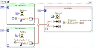
Digital storage oscilloscopes (DSOs) sample analog signals at high rates, convert them to digital data, and store waveforms in memory for detailed analysis. In PCB contexts, this capability is critical for capturing transient events that analog scopes might miss.
Core technical elements relevant to PCB work include:
- High Sampling Rates: Essential for accurately reconstructing fast edges in high-speed digital signals (DDR, SerDes, PCIe) without aliasing.
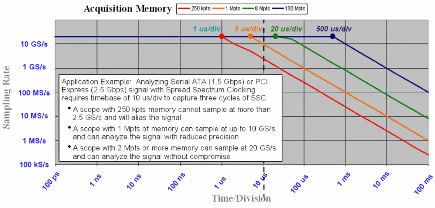
- Deep Memory: Allows long time captures to observe protocol-level behavior or intermittent power rail noise across multiple clock cycles.
- Vertical Resolution: 8-bit to 12-bit or higher ADCs provide the dynamic range needed to measure both low-level noise and high-amplitude signals on the same board.
In manufacturing, DSOs help verify impedance-controlled traces, detect crosstalk, and validate via performance after lamination and drilling.
Key Oscilloscope Features and Their Role in PCB Validation
Modern oscilloscopes offer features specifically valuable for PCB development:
- Advanced Triggering: Edge, pulse width, runt, setup/hold, and serial protocol triggers allow engineers to isolate specific events such as power supply glitches, signal integrity violations, or EMI-induced anomalies on multilayer PCBs.
- Frequency Response Analysis: By combining oscilloscopes with signal generators, engineers perform gain/phase analysis to evaluate filter performance, decoupling networks, and PDN impedance profiles.
- Serial Decoding and Protocol Analysis: Built-in decoding for I2C, SPI, CAN, Ethernet, and high-speed standards helps debug communication buses common in complex PCB designs.
- Spectrum Analysis (FFT): Reveals frequency content of noise and harmonics, critical for EMI/EMC compliance in RF and high-speed digital boards.
These tools directly support Aivon's focus on producing reliable PCBs with tight impedance tolerances and excellent power integrity.
Choosing the Right Oscilloscope for PCB Design and Manufacturing
Selecting an oscilloscope requires balancing several factors based on the target PCB technology:
- Bandwidth: At minimum 3-5x the highest frequency of interest. For today's 5G mmWave and high-speed digital PCBs, 6 GHz to 65 GHz bandwidth scopes are often necessary.
- Sample Rate: Should be 4-5x the bandwidth for accurate waveform reconstruction.
- Channel Count: 4+ channels for simultaneous observation of multiple signals, power rails, and clocks.
- Resolution and Noise Floor: 10-bit or 12-bit models (such as high-precision 65 GHz platforms) provide better insight into subtle noise and jitter on sensitive analog and RF traces.
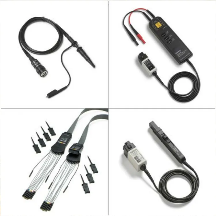
- Probe Quality: Low-capacitance active probes are vital to avoid loading effects that distort measurements on high-impedance PCB nodes.
For Aivon's production environment, we prioritize scopes with excellent long-term reliability, deep memory, and advanced analysis software to support high-volume manufacturing quality gates.
Signal Integrity and Power Integrity Testing with Oscilloscopes
PCB performance at high speeds is often limited by signal and power integrity issues. Oscilloscopes are the primary tool for:
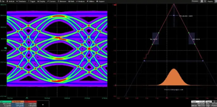
- Measuring rise/fall times, overshoot, ringing, and eye diagrams on critical nets.
- Characterizing power distribution network (PDN) impedance and transient response using step load testing.
- Identifying crosstalk between adjacent traces or layers.
- Validating timing margins in high-speed interfaces where via stub effects or material variations can cause failures.
In multilayer stack-ups, scopes help correlate physical design choices (copper thickness, dielectric materials, via structures) with actual electrical behavior.
Advanced Applications in PCB Manufacturing and Troubleshooting
High-end oscilloscopes support several specialized tasks in PCB production:
- Frequency Response and Bode Analysis: Evaluating filter circuits and decoupling effectiveness directly on the assembled board.
- Jitter and Phase Noise Analysis: Critical for clock distribution networks in 5G baseband and RF PCBs.
- Compliance Testing: Automated mask testing for standards such as USB, PCIe, or Ethernet to ensure boards meet specification before shipment.
- Debugging Handover and RF Issues: Capturing complex modulation waveforms or transient events during simulated 5G/6G operation.
12-bit high-precision platforms are particularly valuable for distinguishing true signal anomalies from instrument noise in low-voltage, high-frequency designs.
PCB-Centric Recommendations for Oscilloscope Usage
When working with complex boards, always:
- Use proper grounding techniques and short ground leads to minimize measurement loop inductance.
- Combine oscilloscope measurements with simulation data for root cause analysis of design issues.
- Perform measurements at multiple production stages - bare board, assembled, and under thermal stress - to catch latent reliability problems.
At Aivon, these practices form an integral part of our quality assurance process, helping us deliver PCBs with outstanding performance in demanding applications such as telecom infrastructure, automotive electronics, and industrial control systems.
Mastering oscilloscope fundamentals and advanced techniques is essential for any organization serious about high-reliability PCB design and manufacturing. The ability to accurately capture and analyze high-speed signals directly influences design success, production yield, and long-term product reliability.
Aivon combines deep PCB manufacturing expertise with rigorous test and measurement practices to produce boards that consistently meet the most challenging signal integrity, thermal, and reliability requirements of today's electronics industry.