The Role of Oscilloscope Probes in PCB Engineering
Accurate signal measurement is fundamental to successful PCB design and manufacturing. Oscilloscope probes directly influence the quality of measurements performed during design validation, prototyping, and production testing. At Aivon, proper probe selection and application are critical for verifying signal integrity, power distribution networks, and high-speed interfaces in complex multilayer boards used in telecom, 5G, automotive, and industrial applications.
Probes serve as the critical interface between the oscilloscope and the PCB. They must transmit the signal with minimal distortion while avoiding excessive loading of the circuit under test. Poor probe selection can introduce measurement errors that lead to faulty design decisions, such as overcompensating for perceived ringing or underestimating crosstalk in high-density layouts.
Key probe characteristics that impact PCB work include bandwidth, input impedance, capacitance, and attenuation ratio. These parameters must align with the target signal frequencies, edge rates, and node impedances found on modern PCBs.
Passive Probe Construction and PCB Applications
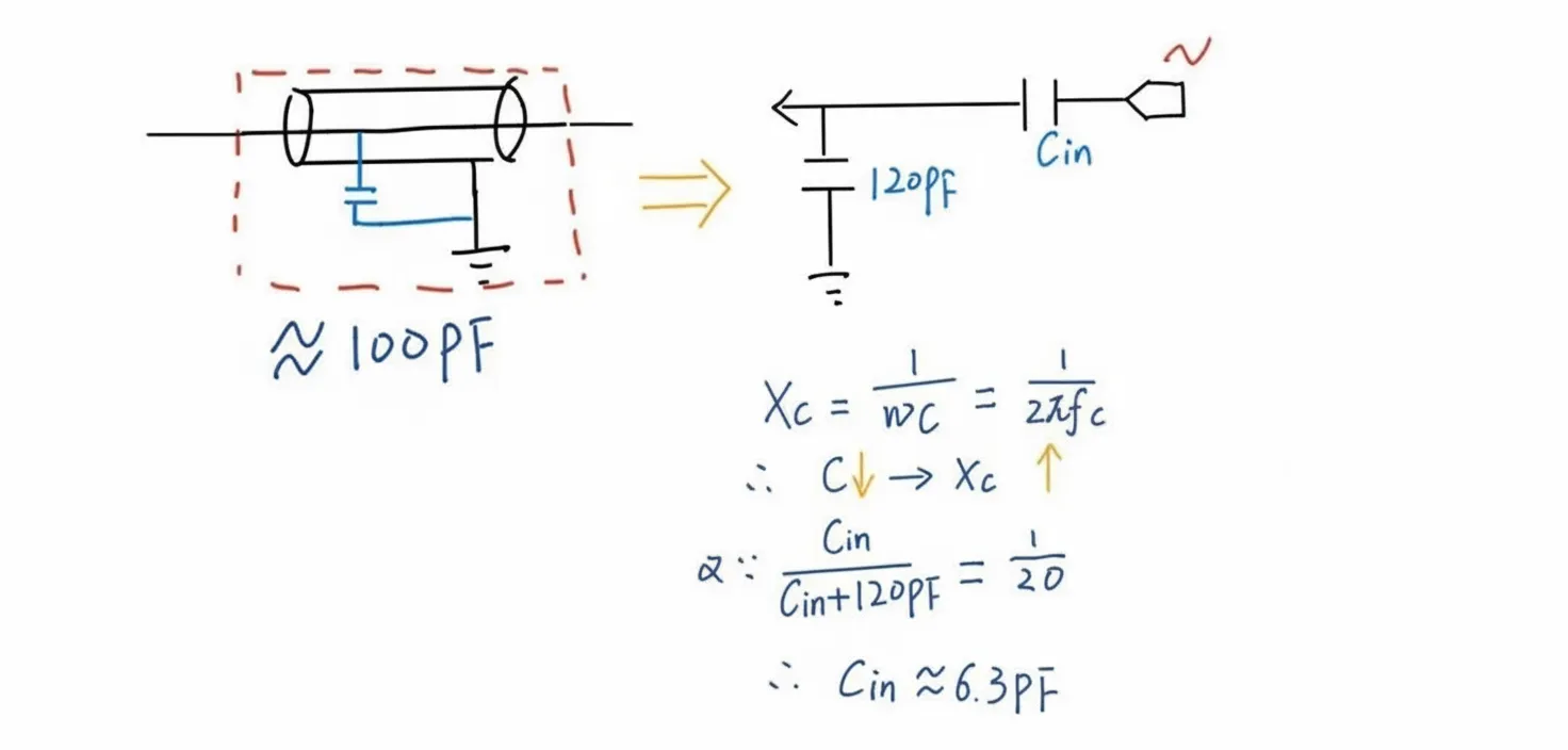
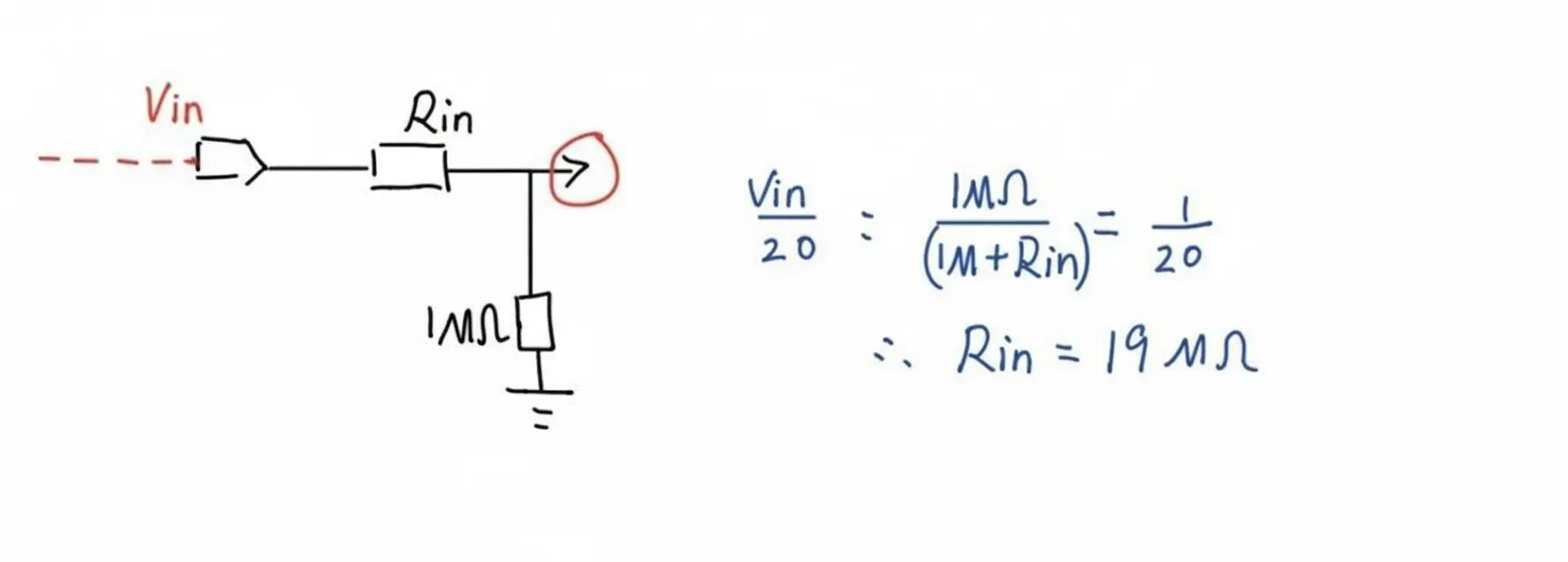
Passive probes are the most common type used in everyday PCB debugging and validation. A typical passive probe consists of a resistive center conductor, parallel compensation capacitor, and a ground lead, forming a compensated voltage divider.
Inside a standard passive probe:
- The probe tip contains a series resistor (usually 9 M ohm) combined with the oscilloscope's 1 M ohm input to create a 10x attenuation.
- A variable compensation capacitor is adjusted to match the cable and scope capacitance, ensuring flat frequency response.
- The ground clip and cable shielding complete the return path.
For PCB manufacturing and design: Passive probes work well for low-to-medium frequency signals and general power rail measurements. Their high input resistance minimizes DC loading, but the relatively high tip capacitance (8-15 pF) can affect high-speed digital signals and sensitive RF traces. In multilayer PCB testing, passive probes are suitable for validating slower control signals, DC-DC converter outputs, and low-speed buses where probe loading remains acceptable.
Active Probes: Superior Performance for High-Speed PCB Designs
Active probes incorporate amplifiers at the probe tip, offering significantly lower input capacitance and higher bandwidth compared to passive probes.
Key Differences Between Active and Passive Probes:
- Input Capacitance: Active probes typically achieve 0.5-2 pF versus 8-15 pF for passive probes, reducing loading effects on high-impedance nodes.
- Bandwidth: Active probes routinely support 1 GHz to 30 GHz+, essential for mmWave 5G, PCIe, DDR, and SerDes interfaces common in advanced PCBs.
- Signal Fidelity: Built-in buffering provides better amplitude accuracy and lower distortion on fast edges.
- Cost and Usability: Active probes are more expensive and usually require power from the oscilloscope, but deliver far superior results on dense, high-speed designs.
In PCB contexts, active probes excel during signal integrity analysis of critical high-speed nets, clock distribution networks, and RF front-end traces where even small parasitic capacitance can cause measurement inaccuracies or mask real design issues.
Instrument Impedance Effects on PCB Voltage Measurements
Oscilloscope input impedance (typically 1 M ohm || 10-20 pF) combined with the probe creates a complex loading network that can significantly alter the actual signal on the PCB.
Important considerations:
- Capacitive Loading: Added probe capacitance slows edge rates and can induce ringing or overshoot that does not exist in normal operation. This is particularly problematic on high-impedance traces or open-drain circuits.
- Resistive Loading: At DC and low frequencies, high probe resistance minimizes impact, but at high frequencies, the capacitive component dominates.
- Ground Lead Inductance: Long ground leads introduce additional inductance, creating measurement artifacts that appear as high-frequency noise. Using spring ground tips or direct PCB ground vias dramatically improves accuracy.
During Aivon's design validation, we account for probe loading in simulations and perform measurements with multiple probe types to distinguish real board behavior from measurement artifacts.
Best Practices for Probe Usage in PCB Manufacturing and Testing
To achieve reliable results when validating PCBs:
- Match probe bandwidth to at least 3-5 times the signal fundamental frequency.
- Use appropriate compensation on passive probes before every critical measurement session.
- Prefer active probes for signals above 500 MHz or on nodes with high source impedance.
- Minimize loop area in the ground return path using short ground springs or coaxial adapters.
- Consider probe loading effects during schematic and layout design phases, potentially adding test points with specific impedance characteristics.
- For high-volume manufacturing, implement automated test fixtures with optimized probe interfaces to ensure consistent quality gates.
Proper probe technique helps identify issues such as via stub reflections, improper stack-up choices, material variations, and power integrity problems before they reach customers. At Aivon, we integrate advanced probing strategies into our full development and production workflow. This commitment ensures that every PCB we manufacture meets stringent signal integrity, timing, and reliability requirements across demanding applications in telecommunications, industrial control, and high-performance electronics.
Mastering oscilloscope probe principles - from passive probe construction to active probe advantages and impedance effects - is essential for any engineering team focused on delivering high-quality, high-speed PCBs.