Spectrum analyzers and vector network analyzers (VNAs) are essential instruments for developing and validating high-frequency printed circuit boards. In RF, microwave, and 5G/mmWave applications, these tools enable precise characterization of signal integrity, EMI/EMC performance, phase noise, and impedance matching. At Aivon, we rely on advanced spectrum analysis and S-parameter measurements throughout our PCB design verification, material qualification, and production quality processes to ensure superior performance in telecom, automotive radar, and industrial RF systems.
Core Applications of Spectrum Analyzers in RF PCB Engineering
Spectrum analyzers measure the frequency domain characteristics of signals on PCBs, making them indispensable for identifying unwanted emissions, harmonics, and noise in high-speed designs.
Key uses in PCB manufacturing include:
- EMI/EMC Debugging: Detecting spurious emissions and radiation from high-speed traces, vias, and connectors that can violate regulatory limits.
- Harmonic Analysis: Evaluating power amplifier and clock circuits for unwanted harmonics that degrade signal quality.
- Signal Purity Verification: Confirming that RF front-end sections meet spectral mask requirements in 5G and mmWave boards.
Modern real-time spectrum analyzers with high dynamic range help PCB engineers correlate layout decisions - such as ground plane stitching, via fencing, and trace routing - with actual electromagnetic behavior.
Phase Noise Measurement Using Spectrum Analyzers
Phase noise is a critical parameter in RF PCB designs, particularly for clock distribution, local oscillators, and 5G baseband systems. Excessive phase noise degrades signal integrity, increases bit error rates, and limits overall system performance.
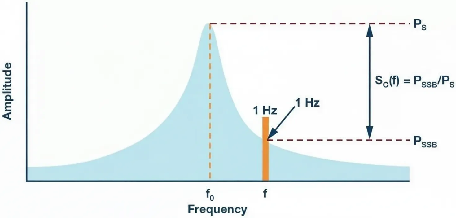
Measurement considerations on PCBs:
- Close-in phase noise analysis requires low-noise power delivery networks and careful isolation between digital and RF sections.
- Spectrum analyzers with dedicated phase noise measurement personalities allow direct evaluation of PLLs, crystal oscillators, and frequency synthesizers integrated on the board.
- PCB material selection (low-loss laminates with stable Dk) and stack-up design significantly influence phase noise performance by minimizing jitter-inducing crosstalk and power supply noise.
In manufacturing, phase noise verification ensures consistent RF performance across production batches, catching issues from material variations or plating inconsistencies.
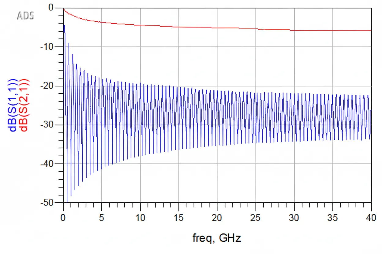
S-Parameters Analysis for Microwave PCB Networks
S-parameters (Scattering parameters) provide complete characterization of high-frequency networks on PCBs, measuring how signals are transmitted, reflected, and coupled between ports.
Critical PCB applications include:
- Impedance Matching Validation: Ensuring 50 ohm transmission lines, vias, and connectors maintain proper matching to minimize reflections.
- Insertion Loss and Return Loss Measurement: Evaluating the impact of copper roughness, dielectric losses, and via transitions on signal propagation.
- Crosstalk and Isolation Analysis: Quantifying coupling between adjacent traces or layers in dense multilayer RF boards.
- De-embedding Techniques: Removing fixture and connector effects to reveal true PCB performance.
Vector network analyzers (VNAs) deliver these measurements with high accuracy, supporting design optimization of complex RF stack-ups and HDI structures.
PNA-X Network Analyzer Advantages for Advanced PCB Characterization
The PNA-X series offers integrated capabilities that extend beyond traditional VNAs, combining spectrum analysis, noise figure measurement, and nonlinear characterization in a single instrument.
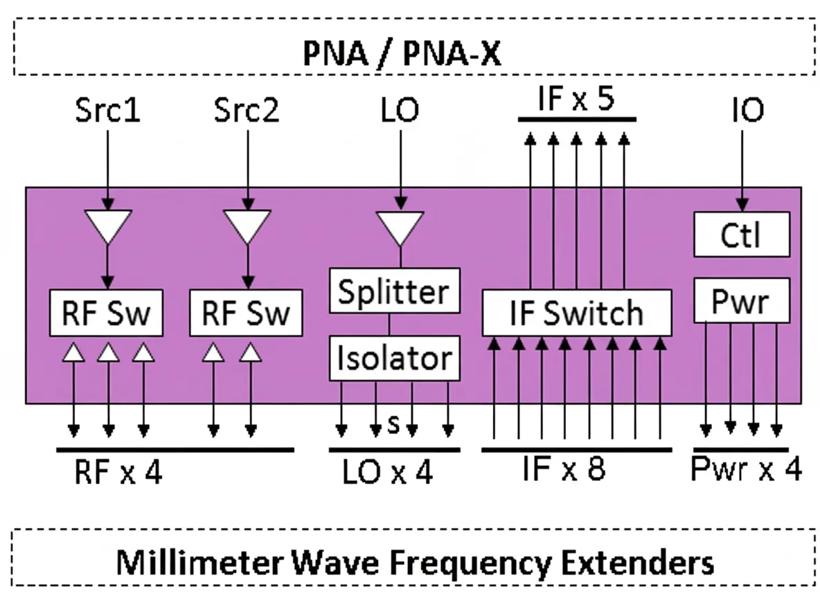
Benefits for PCB engineering:
- Nonlinear Device Testing: Evaluating compression points and intermodulation distortion directly on power amplifier sections of the board.
- Noise Figure Measurements: Critical for low-noise amplifier (LNA) designs in receiver chains, where PCB layout and material losses heavily influence performance.
- Multiport and Balanced Measurements: Supporting differential signaling and complex MIMO antenna arrays common in 5G/mmWave PCBs.
- Time-Domain Analysis: Converting frequency data to time-domain reflectometry (TDR) for identifying impedance discontinuities caused by manufacturing variations.
These capabilities accelerate design iterations and provide deeper insight into real-world PCB behavior under modulated signals.
Superheterodyne Principles in RF PCB Frequency Measurement
Superheterodyne architectures remain foundational in spectrum analyzers and radar systems, using frequency mixing to convert RF signals to a fixed intermediate frequency (IF) for easier processing.
PCB design implications include:
- Local Oscillator Distribution: Low-jitter clock trees and clean power supplies are required to maintain phase stability in down-conversion circuits.
- Mixer and IF Section Layout: Strategic component placement and shielding prevent LO leakage and image frequency interference.
- Filter Integration: Precise control of trace geometry and material properties ensures proper bandpass filtering on the PCB.
In radar and high-frequency test applications, understanding superheterodyne behavior helps optimize PCB layouts for frequency accuracy and spurious-free dynamic range.
PCB Manufacturing and Reliability Considerations
To support effective RF measurement and long-term performance, Aivon focuses on:
- Hybrid material stack-ups combining low-loss laminates (Rogers, Megtron) with standard FR4 for cost-effective RF/digital integration.
- Tight impedance control (+/- 5% or better) and advanced via technologies (back-drilled, stacked microvias) to reduce discontinuities.
- Comprehensive ground plane design with via fencing for superior isolation and EMI suppression.
- Thermal management solutions that maintain stable electrical properties under operational temperature ranges.
- Rigorous validation using spectrum analyzers and VNAs at multiple production stages to ensure consistent quality.
These practices minimize measurement uncertainties and field failures related to signal degradation or electromagnetic incompatibility.
Spectrum analyzers, VNAs, and related RF measurement tools provide the critical feedback loop necessary for successful high-frequency PCB development. From phase noise and S-parameter analysis to EMI debugging and nonlinear characterization, these instruments directly guide decisions on layout, material selection, stack-up configuration, and manufacturing processes. Aivon combines deep expertise in RF PCB manufacturing with advanced measurement capabilities to deliver boards that consistently meet the demanding performance requirements of modern wireless, radar, and high-speed digital systems.