Accurate flow and level measurement plays a vital role in industrial systems where printed circuit boards control critical processes such as cooling, chemical delivery, and environmental monitoring. Whether in PCB manufacturing facilities, automotive thermal management systems, or telecom infrastructure cooling, robust sensor interface designs on PCBs determine measurement reliability, signal integrity, and long-term system performance. At Aivon, we specialize in developing high-reliability PCBs that integrate ultrasonic, differential pressure, and level sensing technologies with superior signal conditioning, EMI immunity, and thermal stability.
Ultrasonic Flowmeter Principles and PCB Integration Challenges
Ultrasonic flowmeters measure fluid velocity using the transit-time difference or Doppler effect of ultrasonic waves passing through a pipe. These non-invasive sensors are widely used in industrial liquid and gas monitoring.
From a PCB perspective, successful integration requires careful engineering:
- Signal Generation and Reception: High-frequency pulse drivers and sensitive receivers demand precise impedance-controlled traces and low-noise amplifier layouts to maintain timing accuracy at microsecond levels.
- High-Speed Signal Processing: Time-of-flight calculations need clean clock distribution and high-resolution ADCs, supported by multilayer stack-ups with dedicated analog and digital ground planes to minimize crosstalk.
- Material Selection: High-Tg FR4 or specialized laminates ensure stable performance across wide temperature ranges common in industrial environments, while controlled dielectric thickness maintains consistent ultrasonic signal conditioning.
- EMI/EMC Protection: Via stitching, guard rings, and strategic component placement prevent external noise from corrupting weak ultrasonic return signals.
Proper PCB design for ultrasonic flowmeters directly impacts measurement accuracy and reliability in applications such as process cooling systems used during PCB lamination and etching.
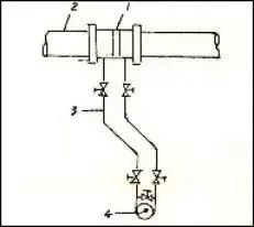
Differential Pressure Flowmeters: Components and PCB Interface Design
Differential pressure (DP) flowmeters, including orifice plates, Venturi tubes, and Pitot tubes, calculate flow rate based on pressure drop across a restriction. They remain popular due to their robustness in harsh industrial conditions.
PCB design considerations for DP flowmeter systems include:
- Pressure Sensor Interfacing: Integration of differential pressure transducers requires low-noise analog front-ends with excellent common-mode rejection and high-resolution ADCs to resolve small pressure differences.
- Signal Conditioning Circuits: Careful layout of instrumentation amplifiers and filtering stages prevents ground loops and thermal drift that could introduce measurement errors.
- Power Integrity: Stable, low-noise power delivery networks are essential, using heavy copper planes and extensive decoupling to support precision analog sections alongside digital processing.
- Installation and Calibration Support: PCBs often incorporate on-board diagnostics and calibration circuitry to maintain long-term accuracy despite vibration, temperature cycling, and contamination.
In PCB manufacturing environments, DP flowmeters help monitor chemical etching solutions and cooling water flow, making reliable sensor PCBs critical for process consistency and yield optimization.
Water Level Measurement Circuits and PCB Implementation
Water level sensing is essential for liquid level control in industrial tanks, cooling systems, and wastewater management. Common methods include ultrasonic, capacitive, and pressure-based techniques.
Key PCB engineering factors for level measurement include:
- Sensor Interface Optimization: Ultrasonic or capacitive level sensors require high-input-impedance amplifiers and noise-filtering circuits to detect small changes in echo timing or capacitance.
- Analog-to-Digital Conversion: High-resolution ADCs combined with proper reference voltage stability ensure accurate level readings across wide ranges.
- Environmental Robustness: Conformal coating compatibility, high-Tg PCB materials, and sealed enclosures protect circuits from humidity, condensation, and corrosive environments typical in fluid monitoring applications.
- Failure Mode Considerations: Redundant sensing paths and watchdog circuitry on the PCB help prevent single-point failures that could disrupt critical cooling or chemical delivery systems.
Manufacturing and Reliability Best Practices for Sensor PCBs
When designing PCBs for flow and level sensing applications, Aivon recommends:
- Hybrid analog-digital stack-ups that isolate sensitive measurement circuits from high-current or switching sections.
- Tight impedance and length matching for timing-critical ultrasonic paths.
- Comprehensive thermal management using copper pours and thermal vias to maintain component accuracy under varying ambient conditions.
- Rigorous testing protocols including thermal cycling, vibration, and EMI immunity validation to ensure long-term reliability.
- Support for industry-standard communication interfaces (4-20mA, Modbus, Ethernet) with robust ESD and surge protection.
These practices reduce measurement drift, improve system uptime, and enhance overall equipment effectiveness in industrial settings.
Flow and level sensing technologies are only as reliable as the PCBs that process their signals. From ultrasonic transit-time analysis to differential pressure signal conditioning and continuous level monitoring, excellence in PCB layout, material selection, and manufacturing directly determines measurement precision and system dependability.
Aivon delivers advanced PCB solutions tailored for industrial sensor integration, helping manufacturers achieve superior process control, higher reliability, and better performance in demanding applications across electronics production, automotive systems, and infrastructure monitoring.