Precise electrical measurements are essential for ensuring power integrity, signal stability, and overall reliability in modern printed circuit boards. Techniques such as the volt-ampere method, current waveform analysis, and ripple voltage measurement allow engineers to validate power distribution networks (PDN), detect manufacturing defects, and optimize designs for high-speed and high-power applications. At Aivon, we apply these measurement methods rigorously throughout design validation, prototyping, and production to deliver PCBs with excellent voltage stability, low noise, and long-term performance for 5G, automotive, and industrial systems.
Volt-Ampere Method for Resistance Measurement on PCBs
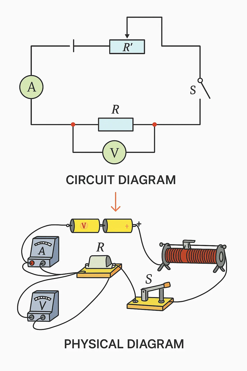
The volt-ampere (V-I) method measures resistance by applying a known current and measuring the resulting voltage drop (R = V/I). This approach is particularly useful in PCB manufacturing for verifying trace resistance, via plating quality, and plane continuity.
In practice:
- A controlled current source injects a stable DC current through the test path while a high-accuracy voltmeter captures the differential voltage.
- Low test currents (mA range) prevent heating effects that could alter readings on thin copper traces.
- This method excels at detecting high-resistance issues caused by incomplete via plating, etching variations, or micro-cracks introduced during lamination and drilling.
For multilayer boards, the volt-ampere technique helps confirm that power and ground planes meet target resistance budgets, directly impacting voltage drop and thermal performance under load.
Current Measurement Methods for Low-Voltage PCB Distribution
Accurate current measurement is critical for validating power consumption, identifying leakage paths, and optimizing PDN designs in low-voltage systems (1.0V-3.3V common in digital PCBs).
Common approaches include:
- Shunt Resistor Method: A precision low-value resistor placed in the current path with differential voltage measurement. Requires careful Kelvin connections to eliminate trace resistance errors.
- Current Probes: Non-invasive tools based on Hall effect, fluxgate, or Rogowski coil principles that measure magnetic fields around conductors without breaking the circuit.
- High-Side vs Low-Side Sensing: Placement decisions affect measurement accuracy and common-mode rejection in complex multilayer stack-ups.
Current Probes offer significant advantages in PCB testing:
- Clamp-on designs allow quick measurements on assembled boards.
- AC/DC probes support both steady-state and dynamic waveform capture.
- High-bandwidth models are essential for observing transient currents in switching regulators and high-speed digital circuits.
These measurements help correlate actual current draw with simulation results, revealing issues such as excessive crosstalk or inadequate copper thickness.
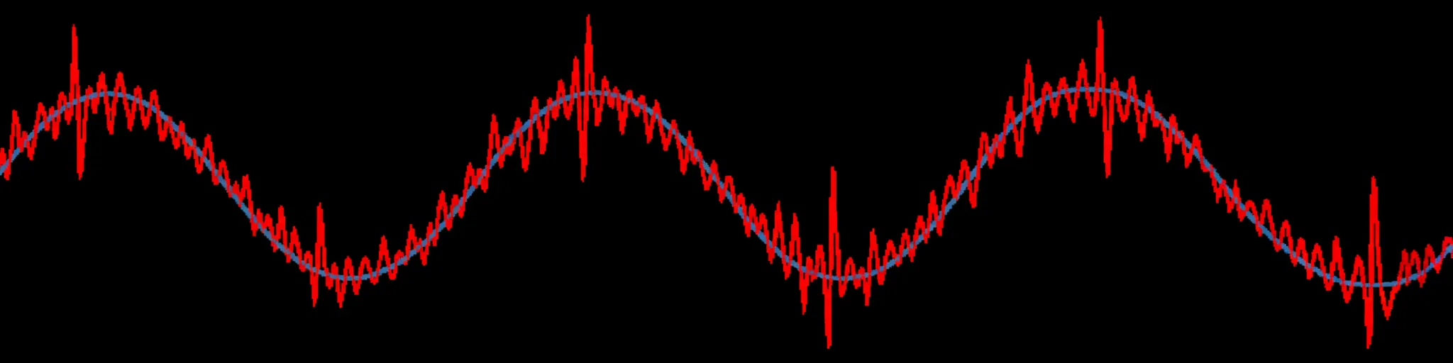
Measuring Output Ripple in DC-DC Converters on PCBs
DC-DC converters are central to PCB power delivery. Output ripple - the AC component superimposed on the DC voltage - must be minimized to prevent noise coupling into sensitive analog, RF, or digital sections.
Effective ripple measurement techniques include:
- AC Coupling on Oscilloscope: Removes the DC offset to focus on noise and ripple components with high vertical resolution.
- Bandwidth Limiting: Using 20 MHz bandwidth limiting to isolate switching ripple from high-frequency noise.
- Probe Technique: Short ground springs and direct probing at the output capacitor to minimize loop inductance that can create false high-frequency artifacts.
High ripple often indicates insufficient output capacitance, poor layout (long feedback traces or inadequate ground return paths), or via inductance issues. In manufacturing, consistent ripple verification ensures that material choices (high-Tg laminates, copper weight) and stack-up configurations deliver stable power under real operating conditions.
Advanced Current Waveform Analysis with Oscilloscopes and Specialized Tools
Oscilloscopes combined with current probes enable detailed dynamic analysis of current waveforms, revealing inrush behavior, switching transients, and periodic noise.
Best practices for waveform capture on PCBs:
- Use low-capacitance current probes or shunt-based sensing with proper compensation.
- Trigger on specific events (load steps, clock edges) to capture rare anomalies.
- Combine voltage and current measurements simultaneously for power quality analysis (P = V x I).
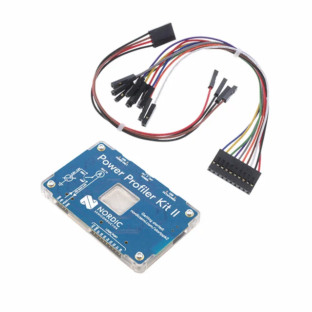
Specialized tools like the nRF PPK2 provide high-resolution current profiling (down to microamp levels) particularly useful for optimizing low-power IoT and battery-operated PCB designs. These instruments help validate sleep-mode currents and identify unexpected leakage caused by component placement or surface contamination during assembly.
Best Practices for Power Integrity Measurements in PCB Production
To achieve reliable results across design and manufacturing stages:
- Perform measurements at multiple points (input, output, critical loads) to map voltage drops and current distribution.
- Account for probe loading and temperature effects on measurements.
- Correlate test data with thermal imaging to identify resistive heating caused by high current density.
- Implement statistical sampling during production to ensure consistent PDN performance across batches.
These techniques support better decisions on copper thickness, thermal via arrays, decoupling strategies, and overall board stack-up.
At Aivon, comprehensive power integrity testing using volt-ampere methods, current probes, ripple analysis, and waveform capture forms a cornerstone of our quality assurance process. This meticulous approach ensures that every PCB we manufacture meets stringent requirements for voltage stability, low noise, and high reliability in demanding applications across telecommunications, automotive electronics, and industrial control systems.
Mastering these measurement techniques is fundamental to producing high-performance PCBs where power integrity directly determines signal quality, thermal behavior, and long-term field reliability.