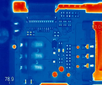
Effective thermal management is critical to the performance, reliability, and lifespan of modern printed circuit boards. Infrared thermography and online thermal cameras provide non-contact, real-time visualization of heat distribution, enabling engineers to identify hot spots, optimize designs, and detect manufacturing defects early. At Aivon, we integrate advanced thermal imaging techniques throughout our PCB design validation, production monitoring, and reliability testing processes to deliver high-performance boards for 5G, automotive, industrial control, and high-power applications.
Principles of Infrared Thermography in PCB Analysis
Infrared thermography detects thermal radiation emitted by objects and converts it into visible temperature maps. All objects above absolute zero emit IR radiation, with intensity proportional to surface temperature and emissivity.
Key system components include:
- Infrared Detector Arrays (often microbolometer or photon detectors) that capture radiation in the 8-14 um long-wave infrared band.
- Optics and Calibration for accurate temperature measurement across varying emissivity surfaces common on PCBs (solder mask, copper, components).
- Signal Processing to generate thermal images with resolution sufficient to detect small temperature gradients on dense boards.
Unlike contact-based methods, IR imaging allows simultaneous visualization of entire PCB assemblies without physical interference, making it ideal for live functional testing and thermal profiling.
Why Online Thermal Cameras Are Essential for PCB Manufacturing
Online (fixed or real-time) thermal cameras provide continuous monitoring during key production and testing stages:
- Hot Spot Detection: Identify localized heating on power planes, high-current traces, or poorly designed thermal vias before failures occur.
- Process Monitoring: Track temperature uniformity during reflow soldering, selective soldering, and press lamination to prevent delamination or component damage.
- Power Integrity Validation: Observe dynamic thermal behavior under varying load conditions to validate copper thickness, plane design, and heat sink integration.
- Early Failure Prediction: Detect abnormal heat patterns caused by voids in vias, insufficient copper pours, or material inconsistencies.
Compared to single-point industrial thermometers, thermal cameras deliver full-field data, significantly improving yield and long-term reliability in high-density HDI and multilayer PCBs.
Common Industrial Temperature Measurement Methods and PCB Relevance
Several thermometer technologies are used in electronics manufacturing, each with distinct advantages for PCB work:
- Infrared Thermometers (Spot Pyrometers): Fast, non-contact point measurements useful for quick verification of component temperatures.
- Thermocouples: High-accuracy contact sensors ideal for precise monitoring during thermal cycling tests and reliability qualification.
- Resistance Temperature Detectors (RTDs): Stable and accurate for controlled environment testing of PCB materials.
- Thermistor-Based Systems: Cost-effective for narrow-range monitoring of specific hot spots.
- Thermal Imaging Systems: Provide the most comprehensive spatial data for complex board analysis.
For PCB applications, combining contact sensors with full-field IR imaging yields the most complete thermal profile, supporting better material selection (high-Tg FR4, metal-core substrates) and stack-up optimization.
Applications of IR Thermography in PCB Design and Reliability
Thermal imaging delivers actionable insights across multiple PCB engineering phases:
- Design Validation: Visualize heat dissipation patterns to optimize component placement, copper weighting, and thermal via arrays before committing to fabrication.
- Manufacturing Quality Control: Detect defects such as insufficient solder joints, delamination, or trapped moisture that manifest as anomalous heating.
- Failure Analysis: Pinpoint root causes of field failures including cracked vias, degraded laminates, or inadequate EMI shielding that increases resistive losses.
- Thermal Cycling and Stress Testing: Monitor boards under accelerated life testing to validate long-term reliability in harsh environments (automotive, telecom infrastructure).
In high-power designs, IR imaging helps confirm effective heat spreading through heavy copper layers and embedded thermal solutions.
Common Faults in Temperature Measurement Instruments and Mitigation
Accurate thermal data depends on properly functioning instruments. Frequent issues include:
- Emissivity Errors: Different PCB surfaces (bare copper vs. solder mask) require correct emissivity settings or corrective techniques.
- Ambient Interference: Reflected radiation or airflow affecting readings - mitigated through controlled testing environments and proper camera positioning.
- Calibration Drift: Regular calibration against blackbody references ensures measurement accuracy for tight-tolerance reliability work.
- Resolution Limitations: Low-resolution cameras may miss small hot spots on fine-pitch components - high-resolution systems are preferred for advanced HDI boards.
At Aivon, we maintain strict calibration protocols and cross-verify thermal imaging data with other measurement methods to maintain measurement integrity.
Best Practices for Thermal Imaging in Professional PCB Manufacturing
To maximize value from infrared systems:
- Establish baseline thermal profiles for each new design under nominal and worst-case conditions.
- Use consistent emissivity corrections and camera settings across production batches.
- Integrate thermal data with electrical test results for comprehensive root cause analysis.
- Combine IR imaging with simulation tools during the design phase to correlate predicted vs. actual thermal behavior.
These practices support better decisions regarding material selection, via design, copper distribution, and overall stack-up configuration.
Advanced thermal imaging is now an indispensable part of high-reliability PCB manufacturing. From early design optimization to production quality gates and post-assembly failure analysis, infrared thermography directly improves thermal performance, reduces field failure rates, and accelerates time-to-market.
Aivon leverages state-of-the-art thermal imaging and temperature monitoring technologies alongside rigorous engineering processes to produce PCBs with superior thermal management, signal integrity, and long-term reliability for the most demanding applications in electronics engineering.