Medical electronics demand exceptional reliability, ultra-low power consumption, signal integrity, and electromagnetic compatibility (EMC). Printed circuit boards (PCBs) serve as the foundational platform that integrates microcontrollers, sensors, power management, analog front-ends, and wireless connectivity while meeting stringent medical safety and performance requirements. Whether for wearable health monitors, infusion controllers, evoked potential stimulators, or mobile diagnostic systems, thoughtful PCB design and manufacturing choices directly determine device accuracy, battery life, patient safety, and regulatory compliance.
Core Challenges in Medical PCB Design
Medical devices operate in noisy environments with tiny biological signals (e.g., ECG, evoked potentials) that are easily overwhelmed by interference. Miniaturization for wearables adds constraints on size, weight, and thermal performance. Key PCB-level challenges include:
- Signal Integrity and Noise Management: Weak analog signals from sensors require careful separation of analog and digital domains. Ground planes must minimize loops, with analog and digital grounds joined at a single low-impedance point near the power entry or ADC reference.
- Power Efficiency: Battery-powered wearables and portables require efficient power distribution, multiple rails, and dynamic management to extend runtime without compromising functionality.
- EMI/EMC Compliance: High-frequency digital circuits and wireless modules can radiate or couple noise into sensitive analog paths. Proper stack-up, shielding, and routing are essential.
- Reliability and Miniaturization: Medical devices often use multilayer boards, HDI (High-Density Interconnect), and controlled-impedance traces for stable performance in compact form factors.
MCU Selection and Integration on PCB
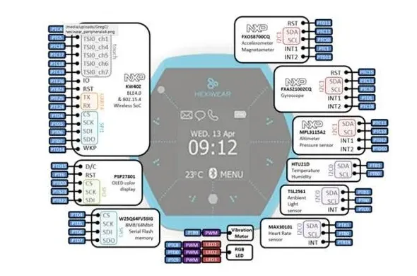
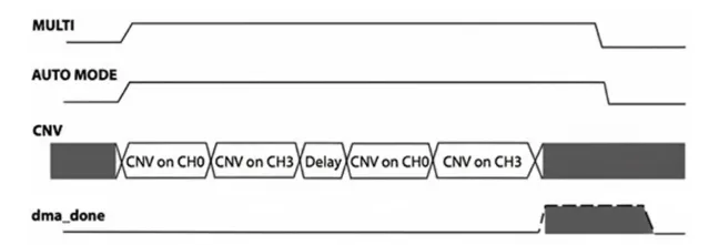
Modern medical designs leverage low-power MCUs such as the ADuCM3029 (ARM Cortex-M3) or platforms like Hexiwear (Kinetis K64F). These integrate ADCs, DMA, and peripherals that simplify PCB layouts while enabling fine-grained power modes.
- Power Management on PCB: Implement buck converters or LDOs with careful capacitor placement to minimize ripple. For devices like the ADuCM3029, route the buck converter path with short, wide traces and low-ESR capacitors to reduce losses at higher VBAT voltages. Use Flexi/sleep modes with peripheral clock gating; dedicate PCB regions for always-on RTC domains.
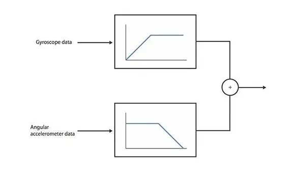
- Sensor Interfaces: I2C, SPI, or dedicated buses (e.g., MikroBUS on Hexiwear) connect motion sensors (accelerometer, gyroscope, magnetometer), optical heart-rate sensors, pressure, temperature, and humidity. Route these traces as differential pairs where possible and shield them from digital noise. For load-cell-based infusion controllers, integrate high-resolution ADCs like the HX711 with stable 5V analog supplies and short analog traces.
PCB stack-up should allocate inner layers for power and ground planes to provide low-impedance returns and reduce EMI.
Analog Front-End and High-Precision Signal Acquisition
Portable ECG or evoked potential systems require low-noise front-end amplifiers. PCB strategies include:
- Separate analog power domains with ferrite beads or filters (e.g., 6.8 µH) to isolate from digital supplies.
- Shield analog sections with copper pours or metal cans.
- Place ADCs close to sensors with short traces to minimize pickup. For evoked potential stimulators (visual/auditory), ensure clean audio codec (e.g., WM8731) routing and stable clock distribution.
Digital filtering (IIR/FIR for 50 Hz notch and low-pass) complements hardware design but relies on clean sampled data from a low-noise PCB.
Thermal Management and Reliability
Medical devices must operate reliably across temperature ranges. Use higher copper weights (2 oz or more) on power planes, thermal vias under high-power components, and materials like high-Tg FR-4 for multilayer boards exposed to body heat or environmental stress. In wearables, optimize component placement to avoid hotspots near skin-contact sensors.
Wireless Connectivity and Data Management
BLE (in Hexiwear), GSM, Zigbee, or Bluetooth modules enable real-time data transmission to smartphones or hospital systems. PCB considerations:
- Dedicated RF layers or co-planar waveguides with controlled impedance.
- Antenna placement away from noisy circuits and ground planes.
- Isolation between RF and analog sections.
Mobile systems benefit from SD card interfaces and EEPROM for data logging, requiring robust power sequencing to prevent corruption.
Manufacturing Considerations for Medical PCBs
Aivon specializes in supporting medical electronics with:
- Multilayer and HDI Fabrication: Essential for compact wearables and high-pin-count MCUs.
- Controlled Impedance: Critical for high-speed signals, clocks, and RF.
- Low-Noise Assembly: Precise component placement, clean soldering, and conformal coating options for reliability.
- Testing and Traceability: In-circuit testing, functional validation, and material certifications aligned with medical standards.
Prototyping benefits from quick-turn services that maintain design intent, while volume production ensures consistent quality for regulatory submissions.
Case Applications and PCB Implications
- Wearables (Hexiwear-based): Hexagonal form factor demands flexible or rigid-flex PCB options, dense sensor integration, and optimized battery routing for motion tracking, fall detection, and cardiac monitoring.
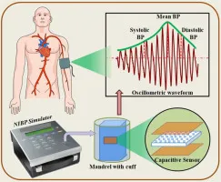
- Infusion Controllers: Load-cell signal chains need stable analog sections; wireless modules require clean power for reliable hospital networking.
- Evoked Potential Systems: FPGA-based designs (e.g., on DE2 platforms) need high-speed I/O routing, clean analog outputs for stimuli, and low-jitter clock distribution.
- Mobile Diagnostic Kits: Integrated ECG, BP, glucose, and temperature functions on a single compact board with efficient power management and touchscreen interfacing.
Best Practices for Medical PCB Success
- Early collaboration between schematic, layout, and manufacturing teams.
- Simulate signal integrity, power integrity, and thermal performance.
- Use ground stitching vias and careful via placement to control impedance and crosstalk.
- Incorporate test points and boundary scan for manufacturability.
- Select materials and finishes (e.g., ENIG) suitable for medical reliability and biocompatibility where needed.
By centering PCB design and manufacturing excellence, developers can transform promising medical concepts into robust, certifiable products that improve patient outcomes and healthcare efficiency. Aivon's expertise in advanced PCB fabrication and assembly provides the reliable foundation these demanding applications require.