Medical digital imaging systems—including digital X-ray, ultrasound, MRI, nuclear medicine, and molecular diagnostics—rely on high-performance printed circuit boards (PCBs) to capture, condition, digitize, and process weak analog signals while maintaining exceptional signal integrity, low noise, and regulatory compliance. As these systems evolve toward higher channel counts, miniaturization, and point-of-care portability, PCB layout, material selection, power distribution, thermal management, and manufacturing processes become decisive factors in image quality, device reliability, and clinical performance.
For PCB manufacturers and design engineers, medical imaging introduces demanding requirements: controlled-impedance routing for high-speed data paths, ultra-low-noise analog front-ends, robust electromagnetic compatibility (EMC), efficient thermal dissipation in compact enclosures, and long-term reliability under continuous operation. Addressing these challenges at the board level enables compact, low-power, and accurate diagnostic equipment that improves patient outcomes across hospitals, clinics, and remote settings.
PCB Design Considerations in Medical Digital Imaging Systems
Medical PCBs for imaging must handle mixed-signal environments where sensitive analog sensor outputs coexist with high-speed digital processing and wireless interfaces. Engineers typically partition the board into isolated analog and digital domains, employing star grounding, dedicated ground planes, and via stitching to minimize noise coupling that could introduce artifacts in X-ray, ultrasound, or nuclear images.
High-frequency traces for ultrasound receive chains or MRI coil arrays require precise impedance control and shielding. Multilayer stack-ups with optimized copper thickness support dense routing for beamforming processors and high-resolution ADCs while keeping overall board thickness suitable for handheld or portable probes. Thermal vias and copper pours dissipate heat from power-hungry FPGAs and processors, preventing drift in temperature-sensitive detectors.
Design-for-manufacturability (DFM) reviews early in the process help ensure reliable via placement, controlled etching tolerances, and surface finishes compatible with medical sterilization and long-term environmental exposure.
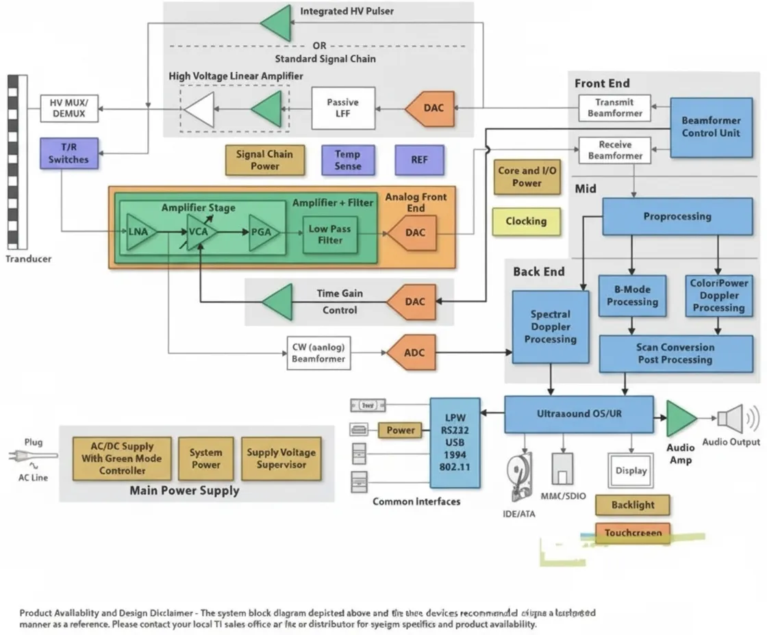
Smart Ultrasound Probes: Transitioning from Cart-Based Systems to Handheld PCB Solutions
The shift from large cart-based ultrasound scanners to compact smart probes demands extreme miniaturization and power efficiency at the PCB level. Modern probes integrate transmit and receive analog front-ends, ADCs, beamforming logic, and data reduction processors directly into the probe housing.
Key PCB challenges include:
- Power management — Switching regulators synchronized below 500 kHz with external clocking minimize interference in the 2–20 MHz ultrasound band while achieving >90 % efficiency in a credit-card-sized footprint.
- Channel density — Highly integrated devices such as 32-channel transmit/receive AFEs enable 64–128 channels within tight power budgets of 3–5 W, eliminating fans and enabling battery operation.
- Data handling — On-board FPGAs or low-power processors perform real-time data reduction before USB 3.1 or wireless transmission, reducing raw data rates from gigabytes per second to manageable streams.
- Size and thermal constraints — Rigid-flex or HDI PCBs allow complex routing in minimal volume while maintaining signal integrity across hundreds of transducer elements.
These PCB optimizations directly enable portable, high-quality imaging for point-of-care, remote, and emergency applications.
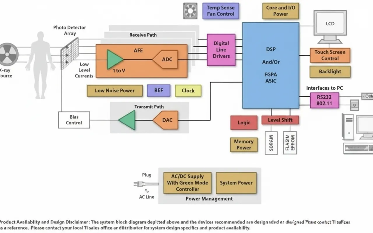
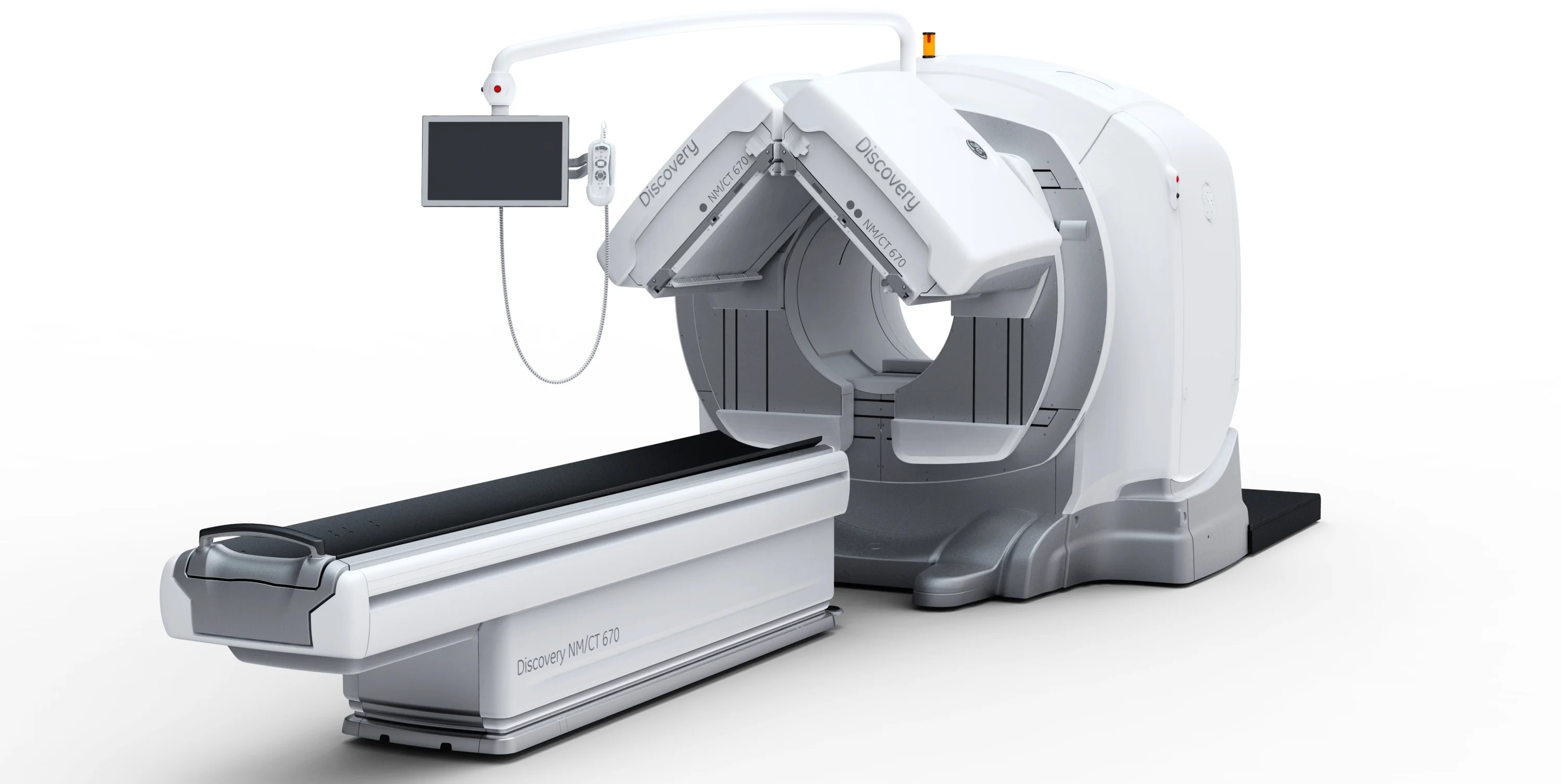
Nuclear Medicine Imaging Devices: Detector Electronics and PCB Reliability
Nuclear medicine systems (gamma cameras, SPECT, and PET) detect gamma photons from radiopharmaceuticals to produce functional images. Detector chains—scintillators, photomultiplier tubes or silicon photomultipliers, preamplifiers, pulse-height analyzers, and correction circuitry—place strict demands on PCB performance.
Low-noise, high-gain analog paths must preserve microvolt-level signals while rejecting electromagnetic interference from nearby digital electronics or hospital environments. Precise grounding, shielding cans, and controlled-impedance routing for high-speed digital outputs after digitization ensure accurate energy discrimination and position encoding.
SPECT and PET systems add rotational mechanics and coincidence detection, requiring robust PCBs that withstand vibration and maintain timing precision across multiple detector modules. Medical-grade laminates, ENIG finishes, and conformal coatings enhance long-term reliability under repeated sterilization and radiation exposure.
Medical Image Processing, Molecular Diagnostics, and Supporting PCB Technologies
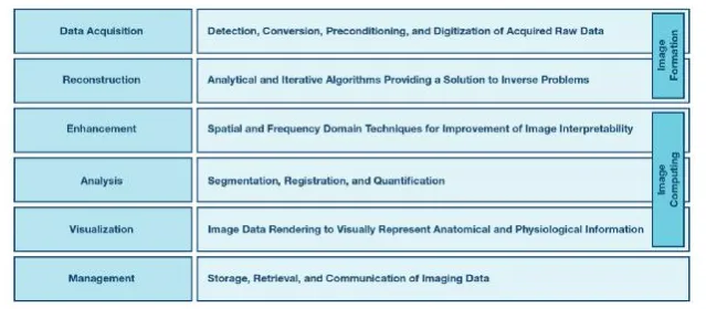
Modern image processing relies on powerful embedded processors and FPGAs for reconstruction, noise reduction, and AI-assisted interpretation. PCBs supporting these functions must deliver high-speed memory interfaces, parallel processing capability, and efficient power delivery to handle large datasets in real time.
In molecular diagnostics, point-of-care analyzers use PCR or LAMP amplification with thermoelectric coolers (TECs) for precise thermal cycling. PCBs integrate high-accuracy temperature sensors (e.g., ±0.1 °C digital sensors), current-drive circuits for TECs, and low-noise optical detection front-ends using current-input ADCs with femtoampere-level noise performance.
Optical detection channels require clean analog routing, minimal leakage currents, and stable power rails to detect faint fluorescence signals early in amplification cycles. Battery-powered designs further emphasize low-quiescent-current regulators and intelligent power sequencing on the PCB.
Manufacturing Excellence, Reliability Assurance, and Future Trends
Medical imaging PCBs undergo rigorous qualification for signal integrity, thermal performance, and EMC compliance with standards such as IEC 60601. Controlled processes for lamination, via filling, and surface finishing ensure consistent performance across production lots. Early collaboration on stack-up design, impedance modeling, and thermal simulation helps avoid common failure modes such as ground bounce, thermal gradients, or EMI-induced image artifacts.
As imaging systems incorporate higher channel counts, wireless connectivity, and AI processing, demand grows for advanced HDI, rigid-flex, and low-power multilayer solutions that meet both performance and regulatory requirements.
Conclusion
Successful medical digital imaging ultimately depends on the quality and sophistication of the underlying PCBs. By prioritizing optimized analog and high-speed digital layouts, robust grounding and shielding, precise thermal and power management, and rigorous manufacturing processes, PCB engineers enable higher image resolution, faster acquisition times, extended device portability, and superior clinical reliability. Collaboration between imaging system developers and specialized medical PCB manufacturers remains essential for advancing ultrasound probes, nuclear medicine detectors, molecular diagnostics, and next-generation digital imaging platforms that deliver accurate, accessible diagnostics worldwide.