5G transport networks - fronthaul, midhaul, and backhaul - form the critical backbone that connects radio units to distributed units, centralized units, and the core network. These segments demand ultra-low latency, massive bandwidth, and exceptional reliability, all of which depend heavily on advanced printed circuit board (PCB) technology. At Aivon, we engineer high-performance PCBs that address the stringent requirements of 5G transport, from high-speed optical interfaces to RF antenna materials and routing hardware.
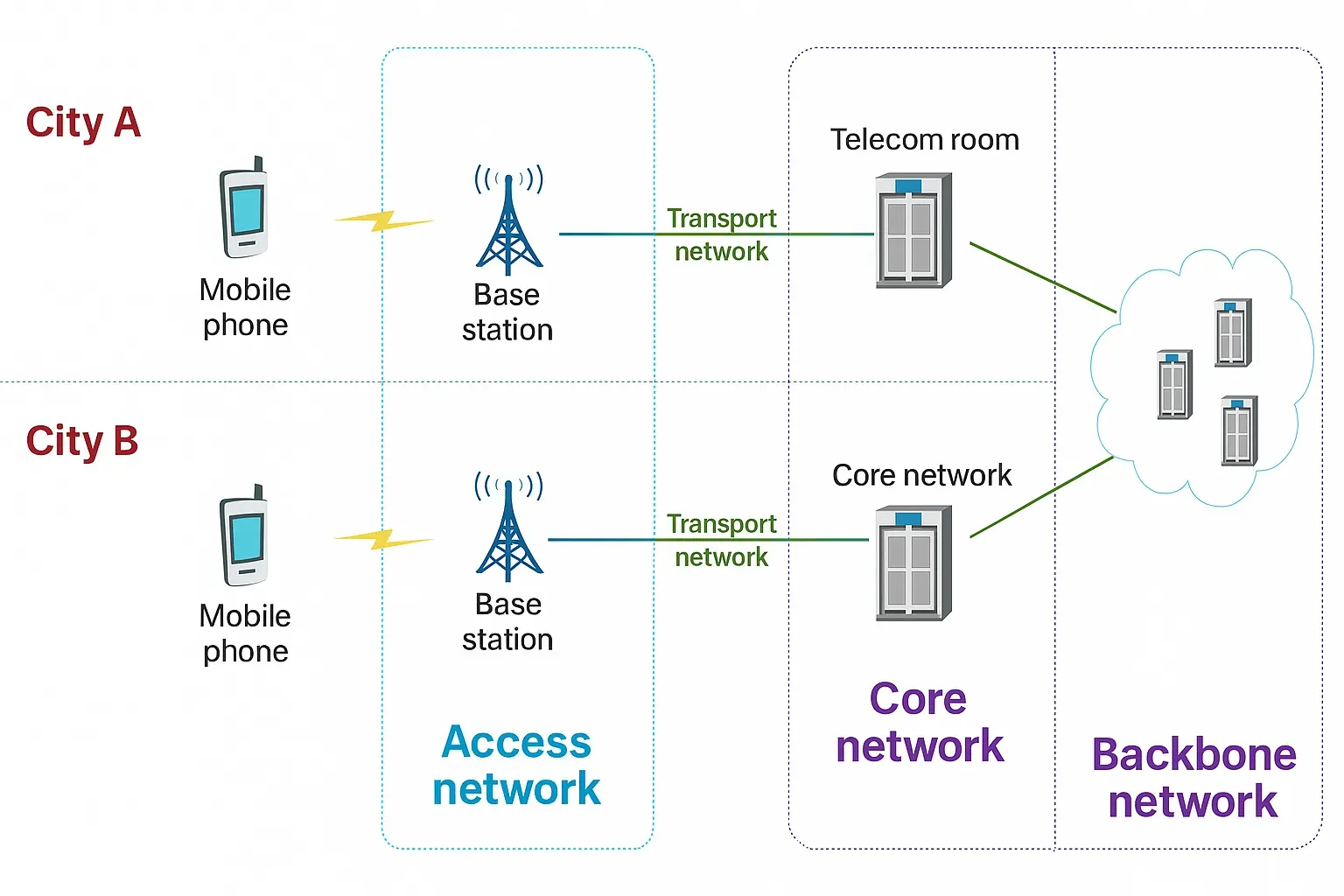
5G Transport Architecture: Fronthaul, Midhaul, and Backhaul Overview
Fronthaul carries raw radio signals between Remote Radio Units (RRUs) and Distributed Units (DUs) using protocols such as eCPRI, requiring extremely high bandwidth and low latency. Midhaul connects DUs to Centralized Units (CUs), while backhaul links the RAN to the 5G core.
PCB implications across these segments include:
- High-Speed SerDes Interfaces: 25G, 50G, and 100G+ serial links demand controlled impedance routing, back-drilling, and low-loss materials to minimize insertion loss and jitter.
- Layer Stack-Up Optimization: Multilayer designs (12-24+ layers) with dedicated high-speed signal layers, solid ground planes, and via stitching for superior signal integrity.
- Power Delivery Networks: Stable, low-noise PDNs capable of supporting high-power optical modules and processors without voltage droops during burst traffic.
Optical Networks in 5G Transport: PCB Integration Requirements
Efficient optical transport relies on Passive Optical Networks (PON) and active WDM systems. Core components - OLT (Optical Line Terminal), ONU (Optical Network Unit), and ODN (Optical Distribution Network) - interface directly with PCBs in base stations and aggregation equipment.
Key PCB design considerations for optical systems:
- Optical Module Integration: High-density layouts supporting QSFP, SFP, and CFP modules with precise impedance matching for high-speed electrical-to-optical conversion.
- Signal Integrity for Long-Reach Links: Low-loss dielectric materials and minimized trace lengths to maintain clean eye diagrams over extended distances.
- Thermal Management: Heavy copper layers and thermal vias to dissipate heat from high-power lasers and PHY chips in outdoor or dense deployments.
- EMI/EMC Control: Compartmentalized shielding and ground plane optimization to prevent interference between optical interfaces and sensitive RF sections.
High-Speed Routing and BGP in 5G Backhaul
BGP (Border Gateway Protocol) remains essential for global IP routing across 5G backhaul networks, enabling efficient traffic engineering and policy-based forwarding between operators and data centers.
PCB-level demands in routing and switching equipment include:
- High-Throughput Packet Processing: Advanced baseband and network processor layouts with wide parallel buses or high-speed serial fabrics requiring tight skew control and crosstalk minimization.
- Timing Synchronization: Low-jitter clock distribution networks critical for precise timing in time-sensitive networking (TSN) and 5G synchronization protocols.
- Scalable Designs: Modular PCBs supporting flexible port configurations while maintaining consistent performance across different backhaul topologies.
Antenna Materials in 5G RF Front-End: LCP vs MPI Characteristics
Antenna performance in 5G small cells and user equipment directly affects transport efficiency. Two leading flexible PCB materials for high-frequency antennas are Liquid Crystal Polymer (LCP) and Modified Polyimide (MPI).
LCP Advantages:
- Extremely low dielectric constant (Dk ~3.0) and dissipation factor (Df ~0.002), ideal for mmWave frequencies with minimal signal loss.
- Excellent moisture resistance and dimensional stability, critical for outdoor base station antennas.
- Superior high-frequency performance supporting wider bandwidths in fronthaul-connected radios.
MPI Advantages:
- Better mechanical flexibility and lower cost for complex 3D antenna structures.
- Good thermal stability but higher Dk/Df compared to LCP, making it more suitable for Sub-6GHz applications.
PCB manufacturing considerations for these materials:
- Hybrid stack-ups combining LCP or MPI antenna layers with standard FR4 or Rogers cores.
- Precise laser drilling and plasma treatment for microvias to maintain signal integrity in flexible-rigid constructions.
- Controlled lamination processes to prevent delamination under thermal stress.
PCB Manufacturing Solutions for 5G Transport Networks
Meeting the combined demands of fronthaul, midhaul, and backhaul requires specialized manufacturing capabilities:
- Hybrid Material Lamination: Combining low-loss materials (Rogers, LCP, Megtron) with cost-effective cores for mixed-signal performance.
- Advanced Via Technologies: Stacked microvias, blind/buried vias, and back-drilling for optimized high-speed routing.
- Tight Impedance Control: +/- 5% tolerances with comprehensive testing to ensure consistent RF and optical interface performance.
- Thermal and Reliability Enhancements: Copper coin embedding, high-Tg materials, and rigorous thermal cycling tests for harsh outdoor environments.
- Signal Integrity Validation: Full VNA and TDR analysis during production to guarantee low-latency transport.
As 5G networks scale, the performance of fronthaul, midhaul, and backhaul increasingly depends on PCB excellence. Superior design directly translates to lower latency, higher capacity, better energy efficiency, and more reliable connectivity across optical transport, routing, and antenna systems.
Aivon provides the advanced PCB manufacturing expertise telecom equipment manufacturers need to build robust, future-ready 5G transport infrastructure, supporting both current deployments and the evolution toward 5.5G and 6G.