5G networks leverage both Sub-6GHz and millimeter wave (mmWave) frequencies to balance coverage and capacity. Each band presents distinct RF challenges that directly impact printed circuit board (PCB) design, material choices, layer stack-up, and fabrication processes. At Aivon, we engineer high-performance PCBs that enable reliable operation across these frequency ranges, supporting modern 5G infrastructure and devices through advanced signal integrity, thermal management, and hybrid construction techniques.
Sub-6GHz Characteristics and PCB Requirements
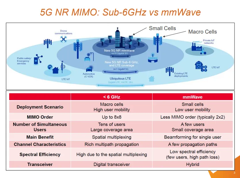
Sub-6GHz bands (primarily 3.3-4.2 GHz in many regions, also known as FR1) offer excellent propagation characteristics, wider coverage, and better penetration through obstacles. These bands support robust mobility and indoor performance but face challenges with spectrum congestion and limited peak bandwidth per channel.
From a PCB engineering perspective, Sub-6GHz designs require:
- Balanced Material Selection: Standard high-Tg FR4 or mid-loss laminates often suffice, with emphasis on consistent dielectric constant (Dk) for impedance control.
- Multilayer Stack-Ups: 8-16 layers typical for integrating baseband, RF front-end, and power management while maintaining isolation between digital and analog sections.
- Power Integrity Focus: Heavy copper layers (2oz-3oz) for high-power amplifiers and efficient thermal vias to dissipate heat from larger coverage-oriented power amplifiers.
- EMI/EMC Optimization: Ground plane stitching and via fencing to control harmonics and spurious emissions in densely populated urban deployments.
5G mmWave Characteristics, Benefits, and Drawbacks
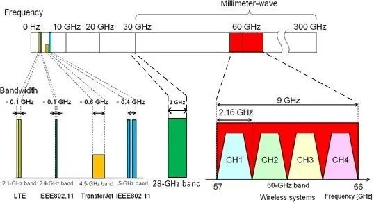
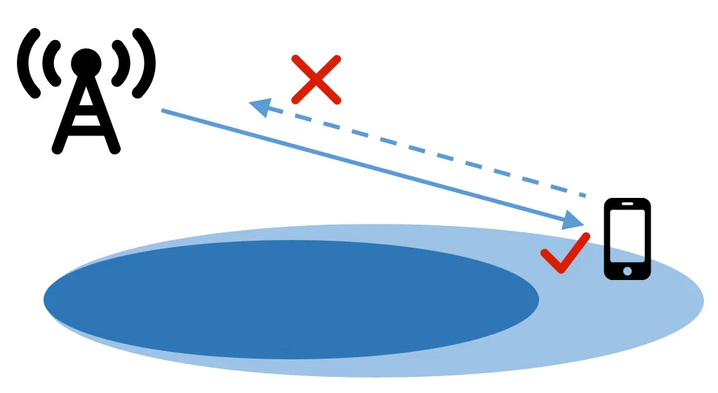
5G mmWave frequencies (24-100 GHz, FR2) deliver massive bandwidth - up to 400 MHz or more per channel - enabling multi-gigabit speeds and low latency. However, they suffer from high free-space path loss, poor penetration, and sensitivity to blockage.
Key PCB challenges in 5G mmWave include:
- Low-Loss Materials Critical: Rogers, Megtron, or other ultra-low Dk/Df laminates are essential to minimize dielectric loss and insertion loss at these high frequencies. Standard FR4 becomes impractical beyond certain thresholds.
- Signal Integrity Demands: Extremely tight impedance tolerances (+/- 5% or better) and short, carefully routed transmission lines to prevent reflections and phase errors in beamforming arrays.
- HDI and Microvia Technology: High-density interconnect designs with stacked microvias are necessary to support massive MIMO antenna arrays (often 16-64+ elements) in compact form factors.
- Thermal Management: Beamforming and high-frequency power amplifiers generate localized heat. Advanced solutions include metal-core PCBs, embedded copper coins, or heavy copper PCBs with optimized via arrays.
Benefits realized at the PCB level include higher spectral efficiency and support for ultra-dense small cell deployments. Drawbacks manifest as increased design complexity, higher material costs, and stricter manufacturing tolerances.
High/Low Frequency Networking in 5G
Modern 5G deployments use dual-connectivity and dynamic spectrum sharing between high (mmWave) and low (Sub-6GHz) bands. This "high/low frequency networking" allows seamless handover and load balancing - leveraging Sub-6GHz for coverage and mmWave for capacity hotspots.
PCB implications for dual-frequency operation are significant:
- Hybrid Stack-Ups: Combining low-loss mmWave layers with cost-effective Sub-6GHz layers in a single board through sequential lamination or hybrid material pressing.
- RF Switching and Filtering: Precise routing for band-switching components and filters, with excellent isolation to prevent inter-band interference.
- Antenna Integration: Support for multiple antenna feeds and tuning networks, often requiring complex ground plane segmentation and via shielding.
- Synchronization and Timing: Low-jitter clock distribution across the PCB to maintain phase coherence between different frequency chains during carrier aggregation or dual connectivity.
Standardization, Spectrum Use, and PCB Production Considerations
5G mmWave standardization by 3GPP has defined specific bands and features like wideband operation and advanced beam management. This drives the need for flexible, future-proof PCB designs capable of supporting evolving spectrum allocations.
Manufacturing challenges include:
- Advanced Fabrication Processes: Laser drilling for microvias, back-drilling for high-speed signals, and plasma treatment for better plating adhesion on low-loss materials.
- Controlled Impedance Manufacturing: Rigorous testing and process controls to maintain performance across production runs.
- Reliability Under Stress: High-Tg materials and enhanced surface finishes (ENIG, ENEPIG) to withstand thermal cycling, vibration, and environmental factors in outdoor small cells or handheld devices.
- Miniaturization Pressure: HDI techniques that reduce layer count while increasing routing density, balancing performance with yield and cost.
PCB Design and Manufacturing Solutions for 5G Success
To overcome the contrasting demands of Sub-6GHz and mmWave, Aivon recommends:
- Hybrid material constructions tailored to specific frequency bands within the same assembly.
- Comprehensive signal integrity analysis and simulation during the design phase.
- Advanced thermal modeling and mitigation strategies for high-power mmWave sections.
- Rigorous RF testing, including S-parameter measurement and passive intermodulation (PIM) testing.
- Scalable production from prototyping to mass volume with consistent quality.
The successful deployment of 5G networks depends heavily on how effectively these frequency-specific challenges are addressed at the PCB level. Whether for base stations, small cells, or user equipment, superior PCB engineering determines real-world performance in coverage, speed, latency, and reliability.
Aivon delivers the specialized PCB manufacturing expertise required to navigate the complexities of 5G mmWave and Sub-6GHz integration, helping telecom manufacturers build more capable and cost-effective wireless infrastructure.