Cellular mobile technology relies on sophisticated radio access systems where the printed circuit board (PCB) serves as the critical backbone. From baseband processing and RF front-ends to advanced waveforms like OFDM and spread spectrum techniques, every aspect of modern 4G/5G performance depends heavily on PCB design, material selection, signal integrity, and manufacturing precision. At Aivon, we support telecom OEMs with high-reliability PCBs engineered for the demanding requirements of next-generation mobile communications.
Core Principles of Cellular Systems and PCB Implications
Cellular networks divide geographic areas into cells served by base stations, enabling frequency reuse, dynamic resource allocation, and seamless mobility through handovers. These principles place stringent demands on device PCBs:
- Frequency Reuse and Interference Management: PCBs must support clean RF signal separation using multilayer stack-ups, ground plane stitching, and via shielding to minimize crosstalk between reused frequencies.
- Mobility and Handover: Rapid cell transitions require stable power integrity and low-jitter clock distribution on the PCB to prevent modem instability during handovers.
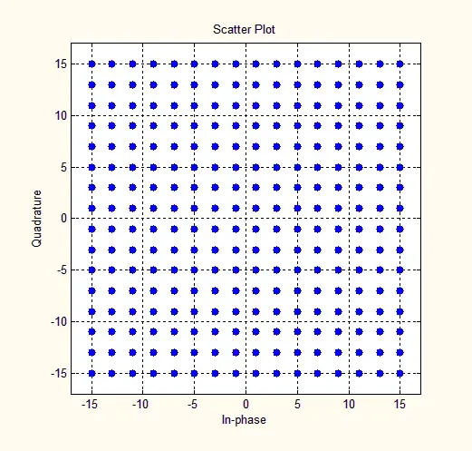
- Multiple Access Technologies: FDMA, TDMA, and CDMA implementations rely on precise impedance-controlled traces and low-loss materials to maintain signal quality across wide bandwidths.
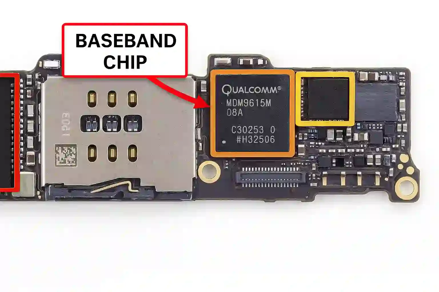
Baseband Processing: From Voice to Digital Domain
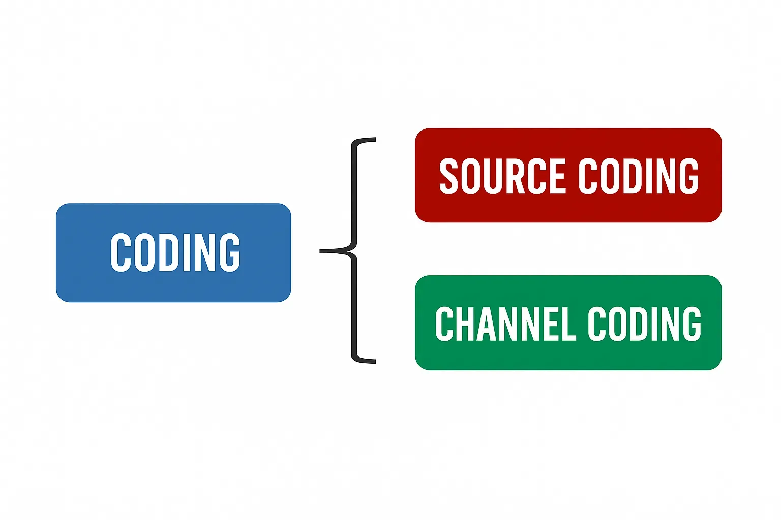
Baseband handles analog-to-digital conversion, source coding, channel coding, encryption, and modulation. In mobile devices, the baseband chipset integrates with the main application processor, making PCB layout pivotal for performance.
Key PCB considerations include:
- High-Speed Digital Routing: Controlled impedance traces for data buses between baseband and memory/storage.
- Power Delivery Networks (PDN): Low-noise voltage regulators and extensive decoupling capacitors to support high-current digital processing without voltage droops.
- Clock Distribution: Low-jitter clocks with minimal skew, achieved through careful layer assignment and guard traces.
- Thermal Management: Baseband processors generate significant heat; thermal vias, copper pours, and high-Tg materials prevent throttling in compact smartphones.
RF Front-End and Upconversion Challenges
After baseband modulation, signals are upconverted to RF carriers for wireless transmission. RF PCBs face unique constraints:
- Impedance Matching: 50 ohm transmission lines with tight tolerances to prevent reflections.
- Low-Loss Materials: Rogers, Megtron, or high-frequency FR4 variants with low Dk/Df to minimize dielectric losses at GHz frequencies.
- Component Placement: Strategic separation of power amplifiers (PAs), low-noise amplifiers (LNAs), and filters to avoid self-desense and EMI issues.
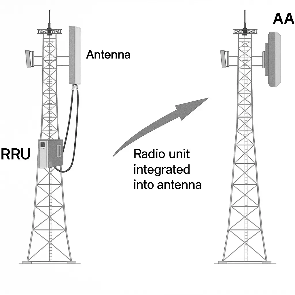
- Antenna Integration: Optimized ground planes and matching networks for maximum radiation efficiency in space-constrained devices.
Upconversion to assigned bands (sub-6 GHz or mmWave) requires excellent phase noise performance and harmonic suppression through precise PCB fabrication.
Spread Spectrum Techniques: DSSS vs FHSS in PCB Context
Spread spectrum improves interference resistance and supports multiple users:
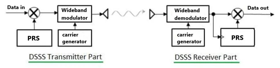
- Direct-Sequence Spread Spectrum (DSSS): Uses high-rate pseudo-noise codes to spread the signal. Requires excellent autocorrelation properties and benefits from PCBs with superior signal integrity to handle wide bandwidth despreading without distortion.
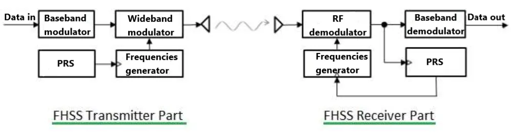
- Frequency-Hopping Spread Spectrum (FHSS): Rapid carrier frequency changes. Demands fast-switching synthesizers and minimal settling time, placing demands on PCB trace length matching and power supply stability.
Modern cellular systems combine elements of both, requiring hybrid RF layouts that support complex modulation while maintaining low EMI.
The Central Role of OFDM in 5G Waveforms
Orthogonal Frequency Division Multiplexing (OFDM) forms the foundation of 5G NR air interface due to its high spectral efficiency and resilience to multipath fading. OFDM divides the channel into many orthogonal subcarriers, each carrying modulated data.
PCB-level implications are significant:
- High Peak-to-Average Power Ratio (PAPR): OFDM signals stress power amplifiers, requiring robust thermal design and high-current copper planes.
- Mixed Numerology Support: 5G allows different subcarrier spacings on the same carrier. This demands flexible RF front-ends and precise filtering on the PCB to manage inter-numerology interference.
- Massive MIMO: Multiple antennas increase routing density, favoring HDI PCBs with microvias for compact, high-layer-count designs.
5G Air Interface and Network Deployment Options
The 5G air interface (NR) introduces flexible numerology, wider bandwidths (up to 400 MHz in FR2), and support for eMBB, URLLC, and mMTC use cases. Deployment options include:
- Non-Standalone (NSA): Leverages existing 4G infrastructure.
- Standalone (SA): Full 5G core and RAN.
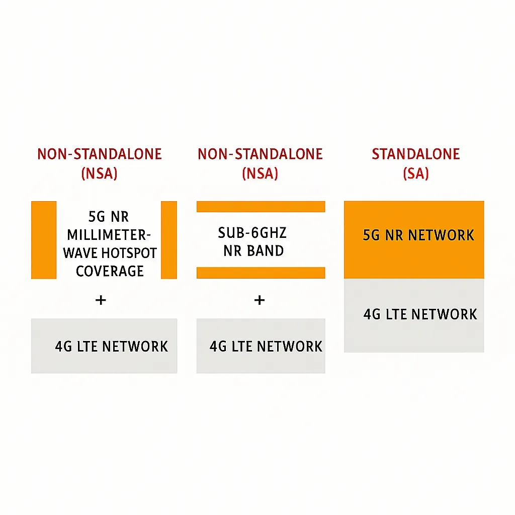
From a PCB perspective, supporting dual-connectivity (4G + 5G) requires complex RF switching, carrier aggregation circuitry, and excellent isolation between multiple antenna paths. FR1 (sub-6 GHz) and FR2 (mmWave) demand different material sets and stack-up strategies.
PCB Manufacturing Solutions for Advanced Cellular Devices
To meet these technical demands, Aivon recommends:
- Multilayer HDI Designs: For high-density baseband and RF integration.
- Impedance-Controlled Fabrication: Tight tolerances for consistent RF performance.
- Advanced Materials: Low-loss dielectrics, heavy copper for power sections, and hybrid stack-ups combining FR4 with high-frequency laminates.
- EMI/EMC Optimization: Via stitching, shielding cans, and careful ground plane design.
- Reliability Enhancements: High-Tg materials, enhanced plating, and rigorous testing for thermal cycling and signal integrity.
These manufacturing capabilities directly translate to better receiver sensitivity, higher transmit efficiency, lower latency, and improved battery life in mobile devices. The evolution of cellular technology from basic voice to high-speed 5G depends fundamentally on excellence in PCB engineering. As waveforms become more complex and spectrum usage more aggressive, superior PCB design and manufacturing become competitive differentiators for device makers. Aivon delivers the advanced PCB solutions needed to power reliable, high-performance mobile communications systems.