IoT devices are prime targets for cybercriminals due to their widespread deployment, often limited computational resources, weak default security, and direct internet exposure. From botnets and data theft to ransomware and physical disruption, attackers exploit these vulnerabilities at scale. Behind effective IoT security - including secure boot, cryptographic protection, cloud integration, AI-driven defense, and future quantum resilience - lies advanced printed circuit board (PCB) technology that enables reliable hardware roots of trust, real-time threat mitigation, and long-term operational integrity.
At Aivon, we specialize in manufacturing high-security PCBs for IoT and connected devices. This article explores why IoT devices attract attacks and examines key security technologies - cloud security differences, AI-based DDoS mitigation, quantum-enhanced approaches, cryptographic modules, CMAC-based secure boot, and MicroSAR network security - all through the lens of critical PCB design, material selection, fabrication, and reliability engineering.
Why Attackers Target IoT Devices: Hardware Implications
IoT devices are attractive because they are numerous, resource-constrained, and frequently deployed with minimal security oversight. Many operate 24/7 with persistent network connections, making them ideal for forming large-scale botnets or serving as entry points into broader networks.
From a PCB perspective, these constraints demand careful engineering:
- Compact form factors require HDI PCBs with blind and buried vias to integrate secure elements, sensors, and wireless modules while maintaining signal integrity.
- Low-power designs must balance energy efficiency with always-on security monitoring, necessitating optimized power distribution networks (PDN) and low-leakage materials.
- Harsh operating environments call for high-Tg laminates, thick copper for thermal dissipation, and robust via structures to withstand temperature cycling and vibration.
Cloud Security vs Traditional Security: PCB Architecture Differences
Cloud security differs significantly from traditional on-premise models by emphasizing shared responsibility, dynamic scaling, and API-based controls. IoT devices often act as edge endpoints feeding data into cloud platforms, requiring strong device-to-cloud authentication and encryption.

This hybrid model drives specific PCB requirements:
- Secure communication interfaces (TLS/DTLS) need controlled impedance routing and low-jitter SerDes channels for reliable encrypted data transmission.
- Integration of hardware security modules (HSMs) or secure enclaves demands isolated power domains and shielded layers to prevent side-channel attacks.
- Edge processing for latency-sensitive security decisions benefits from multilayer boards with dedicated ground planes to reduce EMI in dense IoT deployments.
AI for DDoS Detection and Mitigation: PCB Performance Requirements
AI and machine learning are increasingly used to detect and mitigate DDoS attacks by analyzing traffic patterns in real time. In IoT environments, edge-based AI inference helps filter malicious traffic before it reaches the cloud.
Supporting AI-driven security on IoT devices requires:
- High-bandwidth memory interfaces and efficient neural network accelerators on the PCB.
- Superior thermal management - including thermal vias and optimized copper thickness - to handle continuous inference workloads without throttling.
- Low-noise power delivery to ensure accurate pattern recognition.
Quantum-Enhanced Network Security and PCB Readiness
Quantum computing threatens current cryptographic systems, pushing the adoption of post-quantum cryptography (PQC). IoT devices must prepare for these future threats through hardware agility.
PCB design plays a key role in quantum-ready security:
- Support for new PQC algorithms requires flexible processing architectures with high-speed interconnects.
- Precise clock distribution and signal integrity become critical for timing-sensitive operations.
- Advanced laminates help maintain performance as cryptographic workloads increase.
High-Security Cryptographic Module Design on PCBs
High-security cryptographic modules provide the foundation for encryption, key generation, and authentication in IoT devices.
Effective implementation on PCBs involves:
- Dedicated secure zones with isolated routing and ground shielding.
- High-reliability surface finishes and controlled etching processes.
- Comprehensive power integrity design to protect against power analysis attacks.
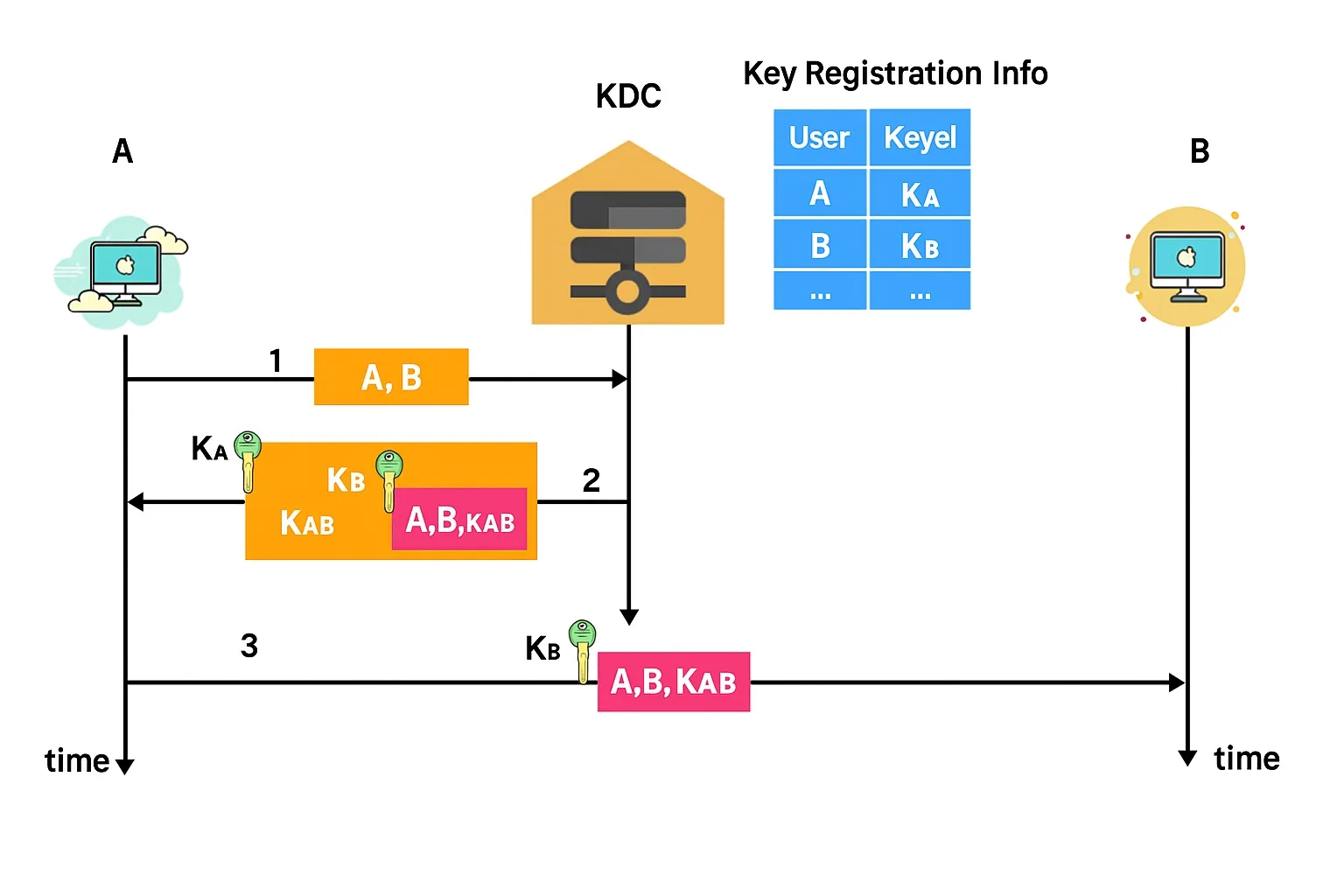
Secure Boot Based on CMAC and Hardware Root of Trust
CMAC enables secure boot by verifying firmware integrity before execution. This hardware root of trust is essential for preventing bootloader-level attacks.
PCB-level considerations include:
- Integration of secure boot controllers with low-latency connections to flash memory.
- Stable voltage rails and decoupling strategies during power-up.
- High-quality lamination and drilling processes to avoid defects that could compromise the boot chain.
MicroSAR Network Security for Automotive and Industrial IoT
MicroSAR provides network security mechanisms tailored for resource-constrained environments. It includes secure onboard communication and firewall-like features. Supporting MicroSAR on PCBs requires optimized stack-ups for Ethernet or fieldbus interfaces, thermal resilience, and redundant design elements.
Best Practices for PCB Manufacturing in Secure IoT Devices
To counter IoT attacks, manufacturers should prioritize:
- Signal Integrity: Controlled impedance and back-drilling for secure interfaces.
- Thermal Management: High-Tg materials and thermal via arrays.
- Power Integrity: Multi-domain PDN design.
- Security Hardening: EMI shielding and automotive/industrial-grade testing.
- Manufacturing Precision: Rigorous DFM and burn-in validation.
Conclusion
Attackers target IoT devices due to their scale and security gaps. Closing these gaps requires robust hardware foundations built on expertly designed PCBs.
From cryptographic acceleration and secure boot to AI-powered defense, the printed circuit board determines IoT security effectiveness. Aivon delivers specialized PCB solutions for secure IoT systems, helping manufacturers build resilient devices.
For expert support on high-security PCB design and manufacturing for your IoT projects, contact the Aivon team to optimize stack-up, materials, and processes for your specific requirements.