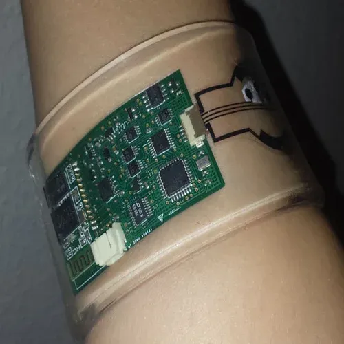
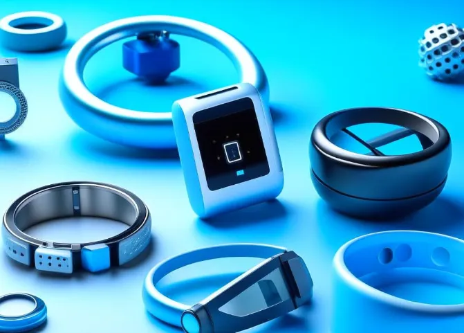
Wearable medical devices have evolved from simple fitness trackers into sophisticated systems that deliver continuous physiological monitoring. At the core of every reliable device lies a carefully engineered printed circuit board that integrates sensors, processors, wireless modules, and power-management circuitry into an extremely compact, flexible, and low-power form factor. Modern designs rely on high-density interconnect (HDI) PCBs, flexible substrates, and advanced stack-ups to achieve the miniaturization, signal integrity, and long-term reliability required for 24/7 skin contact.
Evolution of Wearable Medical Hardware and the Enabling Role of PCB Technology
Early wearable concepts from the 1960s focused on embedding sensors and wireless links into everyday items. Today's devices demand far more: continuous biosignal acquisition, multi-sensor fusion, low-power Bluetooth connectivity, and regulatory-grade safety. These requirements translate directly into PCB-level decisions—multilayer routing for noise-sensitive analog front-ends, microvia technology for dense component placement, and controlled-impedance traces for RF paths.
HDI PCBs enable the fine-pitch component footprints and high layer counts needed to shrink board area while maintaining signal integrity. Flexible polyimide substrates allow the board to conform to body contours, reducing mechanical stress on sensor interfaces and improving user comfort during extended wear.
Critical PCB Design Considerations for Medical Wearables
Designers begin with substrate selection. Thin or flexible laminates with appropriate copper thickness balance bendability and current-carrying capacity. Power-delivery networks must support multi-day operation from tiny lithium-polymer cells, requiring careful decoupling capacitor placement and low-resistance power planes to minimize voltage droop during wireless bursts.
Thermal management is equally vital. Processor and RF modules generate localized heat that must be dissipated without raising skin temperature or corrupting temperature-sensitive measurements. Copper pours, thermal vias, and strategic component placement keep heat away from biosensors. Grounding strategies—star grounding, split planes, and guard traces—preserve the integrity of microvolt-level signals from ECG electrodes or photoplethysmography (PPG) detectors amid motion artifacts and electromagnetic interference.
Material choices extend beyond the board itself. Solder-mask and conformal-coating selections must resist sweat, moisture, and repeated disinfection while maintaining stable dielectric properties over months of continuous use. High-Tg laminates and halogen-free materials further support biocompatibility and long-term reliability in medical environments.
System Architectures and PCB-Level Implementation Challenges
Typical wearable architectures combine a low-power microcontroller, PPG or ECG front-end, accelerometer, wireless transceiver, and battery-management IC on a single rigid-flex or multilayer board. The following constraints drive PCB decisions:
- Miniaturization: Advanced packaging, microvias, and buried vias increase component density while shrinking board size.
- Ultra-low power: Low-quiescent-current ICs are paired with optimized PCB power-distribution networks and sleep-mode routing that isolates always-on sensor paths from high-current wireless sections.
- Reliability and environmental robustness: Robust mechanical stack-ups, reinforced vias, and selective underfill protect against drops, flexing, and moisture ingress. Water-resistant designs often incorporate additional sealing layers around board edges.
- Sensor integration: Multi-sensor fusion requires precise analog signal conditioning on the PCB, with low-noise amplifiers placed close to the sensor contacts to minimize trace length and pickup.
- Connectivity: Low-power Bluetooth and Wi-Fi modules demand controlled-impedance RF traces, proper antenna placement, and EMI shielding to prevent interference with sensitive analog circuits.
Heart-Rate Sensing: PPG Technology and PCB Signal-Conditioning Requirements
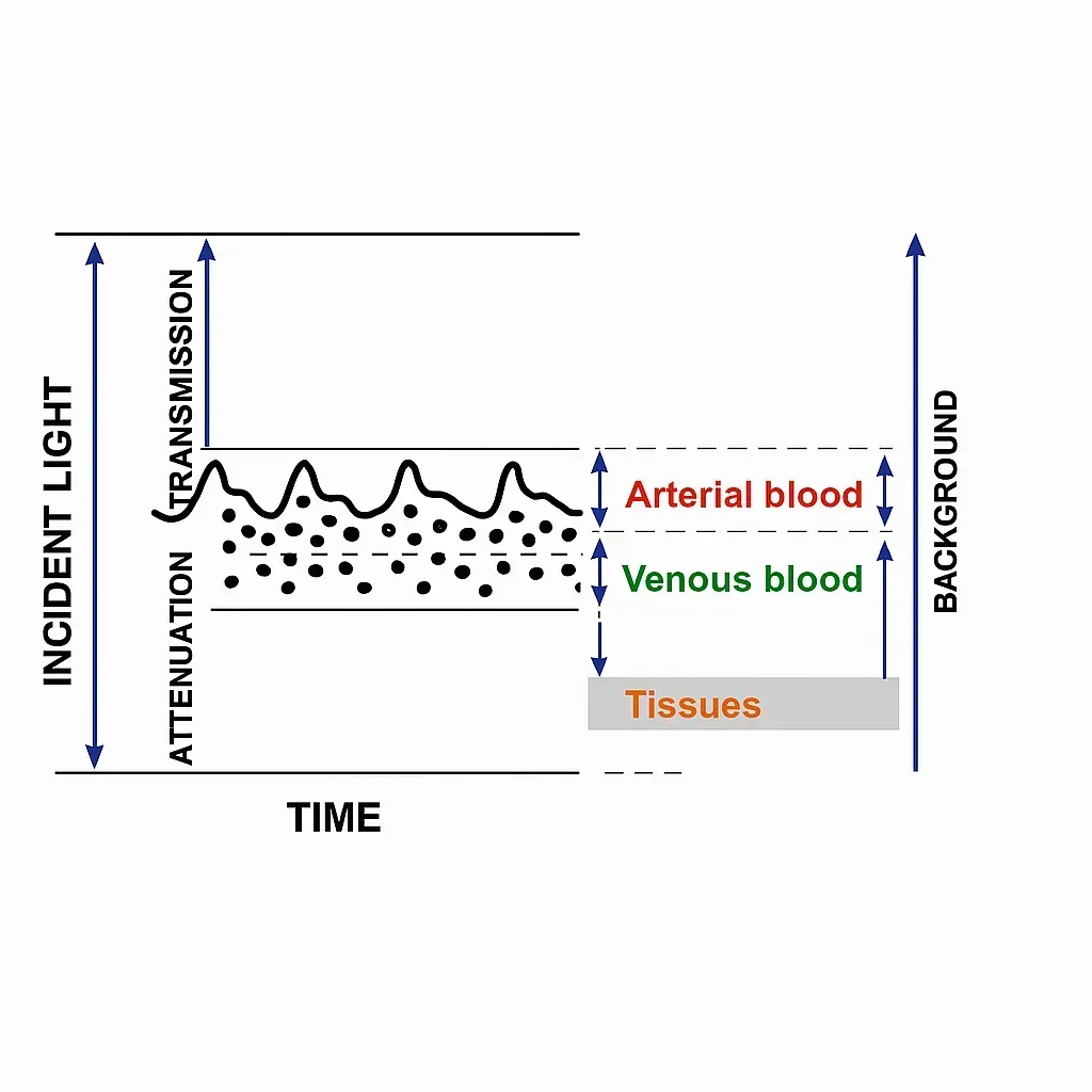
Photoplethysmography remains the dominant heart-rate method in wearables. Green LEDs illuminate the skin; a photodetector captures the reflected light whose intensity modulates with arterial blood volume. The resulting weak, pulsatile signal must be amplified and filtered on the PCB with minimal added noise.
Key PCB considerations include:
- Short, shielded traces between the photodetector and the analog front-end to reduce electromagnetic pickup.
- Dedicated ground planes and guard rings around the sensor area to reject motion-induced artifacts.
- Precise LED drive circuitry with current-matching and temperature compensation to maintain consistent optical output.
- Digital signal processing algorithms running on the microcontroller that compensate for residual motion noise after hardware filtering.
While green LEDs provide strong absorption contrast, sweat or motion can still degrade accuracy. PCB-level improvements—such as differential sensing, adaptive sampling, and tighter integration of the accelerometer for motion compensation—significantly enhance real-world performance.

Safety, Radiation, and Regulatory Compliance at the PCB Level
Concerns about electromagnetic emissions from children’s GPS watches highlight the need for rigorous PCB-level RF design. Short-range wireless transmissions in wearables operate at far lower power than cellular phones, yet improper antenna design, poor grounding, or inadequate shielding can elevate specific absorption rate (SAR) values.
Manufacturers address these risks through:
- Optimized PCB antenna layouts with ground-plane stitching and balun matching.
- EMI shielding cans or conductive coatings over RF sections.
- Strict adherence to regulatory testing for network-access licenses, which impose baseline limits on radiated emissions.
- Material and stack-up choices that minimize unwanted resonances and improve overall electromagnetic compatibility.
Larger, established suppliers typically maintain tighter control over these parameters because brand reputation and supply-chain maturity allow investment in proper PCB simulation, prototype validation, and certification.
Advanced Manufacturing for Long-Term Device Reliability
Producing reliable wearable medical PCBs demands tight process controls: laser-drilled microvias, sequential lamination for rigid-flex constructions, and automated optical inspection to verify fine-line integrity. High-volume medical-grade production further requires traceability, clean-room assembly, and accelerated life testing that simulates repeated flexing, temperature cycling, and moisture exposure.
Companies that outsource critical PCB fabrication to experienced manufacturers gain access to advanced capabilities—such as impedance-controlled routing, buried capacitance layers, and biocompatible surface finishes—without maintaining in-house expertise. This partnership approach directly improves device performance, regulatory compliance, and long-term field reliability.
By anchoring every design decision in PCB engineering principles—material selection, layout topology, thermal and signal integrity, and manufacturing process capability—developers can deliver wearable medical devices that are smaller, more accurate, safer, and more durable. The result is hardware that meets both clinical expectations and consumer demands for continuous, comfortable health monitoring.
Future Trends in PCB Technology for Next-Generation Wearable Medical Devices
The next wave of wearable medical devices will be defined by breakthroughs in printed circuit board architecture that enable smaller form factors, higher sensor density, and true long-term biocompatibility.
Stretchable and skin-conformable electronics are moving from research to production. Hybrid constructions that combine rigid islands for active components with ultra-thin, elastomeric interconnect layers allow the PCB to stretch and recover with skin movement. This eliminates mechanical stress on solder joints and sensor contacts, enabling multi-week or even multi-month continuous monitoring patches for ECG, EEG, and glucose tracking.
Embedded-component and ultra-high-density interconnect (UHDI) technologies with line/space below 20 µm are becoming mainstream. By burying active dies and passive components inside the PCB stack-up, designers achieve board thicknesses under 0.4 mm while increasing routing density. This directly supports the miniaturization required for next-generation smart rings, earbuds, and implantable-adjacent wearables.
On-board edge AI is driving new PCB power and thermal strategies. Dedicated neural processing units integrated into the board require isolated power domains, high-speed memory routing, and advanced thermal vias or heat-spreaders to maintain safe skin-contact temperatures during continuous inference. These capabilities allow real-time arrhythmia detection or sleep staging without cloud latency.
Advanced substrate materials are entering volume production. Liquid-crystal polymer (LCP) and modified polyimide films deliver superior high-frequency performance for future 5G/6G and UWB connectivity, while graphene-enhanced copper foils improve thermal spreading. At the same time, bio-based and partially biodegradable laminates are being qualified to meet emerging sustainability and end-of-life regulations without compromising electrical or mechanical reliability.
Wireless power transfer and multi-modal energy harvesting are now being designed at the PCB level. Optimized coil layouts, rectenna integration, and piezoelectric or thermoelectric harvesters embedded in the board stack-up enable devices to operate for months on minimal user intervention, significantly improving patient compliance.
Hardware-rooted security is becoming a standard PCB requirement. Secure elements, physical unclonable functions (PUFs), and encrypted data paths are implemented directly in the board layout to protect physiological data from the point of acquisition through wireless transmission.
Conclusion
Wearable medical devices achieve clinical value only when their printed circuit boards are engineered with equal attention to miniaturization, signal integrity, thermal performance, mechanical durability, and regulatory compliance. Every advance in device capability—from higher sensor accuracy to longer battery life and greater user comfort—ultimately rests on precise PCB material selection, stack-up design, layout topology, and manufacturing process control.
As the industry shifts toward stretchable electronics, on-board AI, sustainable materials, and hardware-level security, manufacturers that master these PCB-level innovations will set the standard for the next generation of reliable, safe, and intelligent wearable healthcare technology.