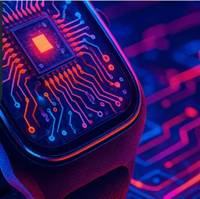
Smart wristbands have evolved into compact wearable systems that combine activity tracking, sleep monitoring, heart-rate sensing, and wireless connectivity within a form factor that must endure daily flexing, moisture exposure, and constant motion. From a PCB manufacturing perspective, these devices demand highly optimized boards that balance miniaturization with signal integrity, thermal performance, and electromagnetic compatibility.
Core Functions and Their PCB Implications
Modern smart wristbands rely on integrated sensors and low-power electronics to deliver step counting, distance estimation, calorie tracking, sleep-stage analysis, vibration alerts, and Bluetooth data synchronization. These functions place strict requirements on the underlying PCB.
Activity monitoring depends on precise accelerometer placement and clean analog signal paths. Sleep tracking and heart-rate measurement require stable power rails and minimal noise coupling to avoid inaccurate readings during movement. Vibration motors and wireless modules introduce additional demands on power distribution and RF performance. Water resistance further necessitates careful material selection and protective coatings to prevent corrosion at the board level.
PCB Layout and Routing Guidelines for Compact Wearables
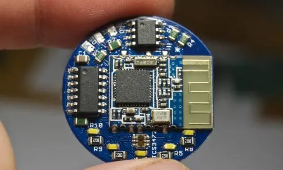
Smart wristband PCBs are typically four- or six-layer designs using single- or double-sided SMT assembly to fit within a slim, flexible enclosure. Effective partitioning separates digital, analog, RF, and high-frequency PCB sections to minimize crosstalk and maintain reliable wireless communication performance.
Clock and crystal circuits must follow the shortest possible paths to their target devices, with copper pours or guard rings providing shielding. Critical traces benefit from copper clearance around crystal areas and avoidance of crossing data lines. Sensor modules using analog circuitry are best treated as discrete blocks that communicate via well-defined interfaces, reducing integration complexity.
Power management is critical because of the small battery capacity and expectation of multi-day operation. Short, wide traces for high-current paths and strategic decoupling capacitor placement help maintain stable voltage levels during Bluetooth transmission or sensor bursts.
EMC Design Considerations for Wearable Smart Bands
Dense component packing in wristbands makes electromagnetic compatibility a primary design driver. Common issues include unstable Bluetooth pairing, sensor interference from high-frequency noise, and electrostatic discharge (ESD) vulnerability at charging ports.
Designers address these through targeted filtering: TVS diodes and magnetic beads on power inputs, PI-type filters on accelerometer supplies, and high-frequency beads on Bluetooth rails. Ground planes are often split or referenced separately for digital, analog, and RF domains, with 0-ohm jumpers providing controlled connections where needed. Signals crossing ground splits are avoided to prevent large loop areas that attract external interference.
A continuous ground pour around the board edge, combined with recessed critical traces, reduces ESD coupling through enclosure gaps. Mechanical sealing and increased spacing around buttons further enhance tolerance to real-world discharges.
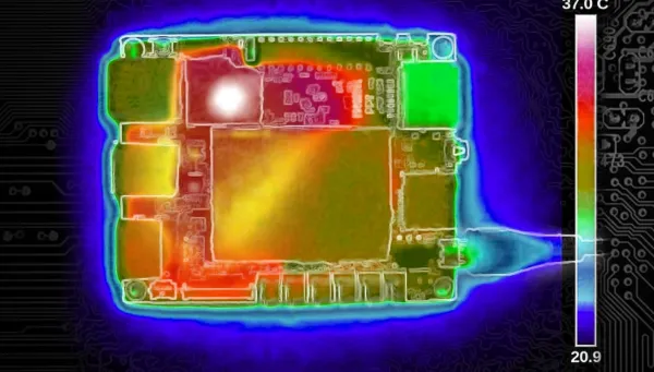
Thermal Management and Material Choices in Wristband PCBs
Processor and charging circuits generate localized heat that must be dissipated without increasing band thickness. Thermal vias, thicker copper layers, and strategic component placement move heat away from the skin contact area. Flexible or rigid-flex substrates are frequently chosen to accommodate the wrist's curvature while maintaining trace integrity under repeated bending.
High-Tg materials and moisture-resistant coatings improve long-term reliability in environments involving sweat and occasional water exposure. These choices directly influence both manufacturing yield and field performance.
uilding Reliable Smart Bands: Manufacturing and User Value
From a manufacturing standpoint, consistent step-count accuracy and sleep-stage detection depend on tight control of sensor placement tolerances, trace impedance, and ground integrity during fabrication. Variations in PCB stack-up or via quality can introduce measurement drift that users quickly notice.
When evaluating whether a smart band delivers lasting value, engineering teams focus on factors such as battery life, sensor repeatability across devices, and the robustness of wireless performance. Devices that maintain accurate data over extended wear periods and survive daily mechanical stress provide clearer benefits for users seeking motivation through quantified activity and sleep insights.
Conclusion
Successful smart wristband development hinges on PCB-level decisions that simultaneously support dense functionality, low power consumption, and robust EMC performance. By prioritizing careful partitioning, targeted filtering, thermal vias, and appropriate substrate selection, manufacturers can produce wearables that deliver reliable data while withstanding real-world use conditions. These engineering practices ultimately determine whether a device remains useful beyond the initial novelty period.