











PCB Specifications
| Parameter | Value | Parameter | Value |
|---|---|---|---|
| PCB Type | Flexible PCB | Quantity | 20 pcs |
| Layers | 4 Layers | Board Type | Single PCB |
| Dimensions | 26.6 x 235 mm | Copper Weight | 1/3OZ |
| Thickness | 0.23 mm | Min Track / Spacing | 6/6mil↑ |
| Surface Finish | ENIG (Immersion Gold) | Min Hole Size | 0.3mm↑ |
| Solder Mask | Black | Silkscreen | White |
| Material | Rolled Copper | Stiffener | None |
Manufacturing Timeline
Logistics Information
Key Manufacturing Processes
Manufacturing Summary
This 4-layer flexible PCB order consisted of 20 single boards measuring 26.6 × 235 mm with an overall thickness of 0.23 mm. Rolled copper at 1/3 oz weight was selected to preserve pliability, paired with 0.3 mm minimum holes, standard 6/6 mil trace spacing, black solder mask, white silkscreen, and immersion gold ENIG finish. No stiffeners were required, allowing the full length to remain dynamically flexible.
Polyimide material handling began the sequence to avoid surface marks or creases on the thin substrate. Inner layer imaging and etching were followed by precise stack alignment and high-pressure lamination. Coverlay lamination was then applied to protect the conductors while maintaining the required bend radius across the narrow, elongated format.
Electroless nickel and immersion gold deposition provided stable pad surfaces, after which dynamic flex testing and electrical testing confirmed consistent performance. The complete run was executed in 10 days, delivering boards that met all dimensional and electrical criteria without deviation.
Explore More PCB Manufacturing Resources
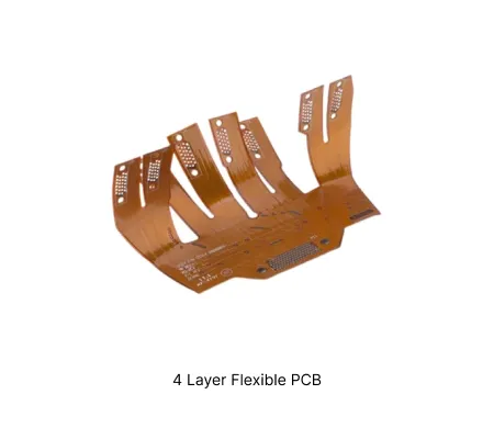
4 Layer Flexible PCB Manufacturing Insights
Discover how AIVON manufactures 4 Layer Flexible PCBs, including multilayer flexible circuit structures, layer alignment control, bending performance, manufacturing challenges, and real production experience from customer orders.
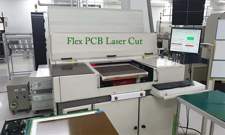
Mastering Flexible PCB Manufacturing: Handling Thin and Bendable Substrates
Learn about flexible PCB manufacturing equipment designed for handling thin, bendable substrates. Gain insights into laser cutting, adhesive bonding, and testing methods to ensure precision and reliability in production.
Real Production Records
| Order ID | PCB Type | Layers | Dimensions | Solder Mask | Surface Finish | Quantity | Action |
|---|---|---|---|---|---|---|---|
| FPC-20260821-065 | Flexible PCB | 4 | 111.25 x 16.75 | Yellow | ENIG (Immersion Gold) | 5 | View detail |
| FPC-20260819-026 | Flexible PCB | 4 | 59.8 x 65.5 | Yellow | ENIG (Immersion Gold) | 25 | View detail |
| FPC-20260810-032 | Flexible PCB | 4 | 357 x 45.8 | Black | ENIG (Immersion Gold) | 1000 | View detail |


