











PCB Specifications
| Parameter | Value | Parameter | Value |
|---|---|---|---|
| PCB Type | Flexible PCB | Quantity | 10 pcs |
| Layers | 4 Layers | Board Type | Single PCB |
| Dimensions | 285 x 40 mm | Copper Weight | 1/3OZ |
| Thickness | 0.2 mm | Min Track / Spacing | 3/3mil |
| Surface Finish | ENIG (Immersion Gold) | Min Hole Size | 0.3mm↑ |
| Solder Mask | Yellow | Silkscreen | White |
| Material | Rolled Copper | Stiffener | FR4 Stiffener |
Manufacturing Timeline
Logistics Information
Key Manufacturing Processes
Manufacturing Summary
Manufacturing this batch of 4-layer flexible PCBs involved a 0.2 mm thin stackup using 1/3 oz rolled copper and 3/3 mil trace spacing across the narrow 285 × 40 mm single-board format. The specification included yellow soldermask, white silkscreen, FR4 stiffeners in designated areas, and immersion gold ENIG finish. Impedance characteristics were addressed through stackup engineering and confirmed with TDR testing, requiring exact registration on the thin polyimide material.
Material preparation and inner layer imaging were followed by trace width compensation during etching to achieve the target geometries. Layer stack alignment, high pressure lamination, coverlay application, and solder mask processing were sequenced to protect the flexible layers. We performed dynamic flex testing alongside full electrical testing, verifying both mechanical endurance and circuit integrity across all 10 boards.
Completed over 12 days, the run produced consistent results that met every tolerance for this impedance controlled flexible PCB. The combination of fine features, light copper weight, and non-standard mask color on such a thin construction demanded precise process control at each stage.
Explore More PCB Manufacturing Resources
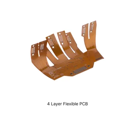
4 Layer Flexible PCB Manufacturing Insights
Discover how AIVON manufactures 4 Layer Flexible PCBs, including multilayer flexible circuit structures, layer alignment control, bending performance, manufacturing challenges, and real production experience from customer orders.
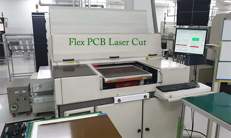
Mastering Flexible PCB Manufacturing: Handling Thin and Bendable Substrates
Learn about flexible PCB manufacturing equipment designed for handling thin, bendable substrates. Gain insights into laser cutting, adhesive bonding, and testing methods to ensure precision and reliability in production.
Real Production Records
| Order ID | PCB Type | Layers | Dimensions | Solder Mask | Surface Finish | Quantity | Action |
|---|---|---|---|---|---|---|---|
| FPC-20260821-065 | Flexible PCB | 4 | 111.25 x 16.75 | Yellow | ENIG (Immersion Gold) | 5 | View detail |
| FPC-20260819-026 | Flexible PCB | 4 | 59.8 x 65.5 | Yellow | ENIG (Immersion Gold) | 25 | View detail |
| FPC-20260810-032 | Flexible PCB | 4 | 357 x 45.8 | Black | ENIG (Immersion Gold) | 1000 | View detail |


